Introduction
I’ve received a request to talk about caches, which is a topic near and dear to my heart. In fact, my Ph.D. dissertation was a rather lengthy book on the topic. The last I checked, my old research group was still hosting an html version of my dissertation here.
I’ll get to caches in my next article, but, as I often say in my current profession, I think it would be helpful to first ”lay a foundation.”
To understand the purpose of caches and to understand why they are designed the way they are designed, you first need to know just a little bit about memory.
What is Memory?
The term “memory” is used, in CPU design, to refer to a circuit that “maintains state.” What that means is, essentially, that memory is a circuit that maintains its value (it’s “state”) for some period of time, regardless of what you do to the inputs of the circuit.This is to be contrasted with the logic gates I discussed in earlier articles in this series. An inverter, of example, changes its value if you change the value of its input. If the input changes to a logic 0, then the output changes to a logic 1. And vice versa. As soon as you change the value of the inputs, the value of the output begins to change.
When you have a memory circuit, however, you can control when the outputs are allowed to change. Typically, memory circuits have some sort of method of storing a value, and some mechanism that permits reading that value. There is also a mechanism that permits you to change the value that is stored in the memory.
Memory is used in many ways in modern computer systems. The most important purpose of memory is to hold the instructions that the CPU needs to execute, and to hold the data upon which the CPU performs computations, and the results of those computations.
For example, consider a small program written in some generic computer language, that looks like this:
At a high level, this code is using several memory locations to hold data, and at least two memory locations to hold instructions. The variables tax, total, and tax_rate are each stored in memory somewhere. Each of the two instructions - the multiplication and the addition - are also stored in memory.
The first instruction fetches (or “loads”) data from two different memory addresses, one for total and one for tax_rate. These two items of data are multiplied by the CPU and then the result, tax, is placed (or “stored”) in memory.
The second instruction means the CPU needs to fetch total and, after modifying it by performing an addition, needs to store it in memory again.
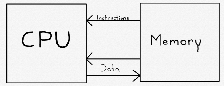
Most CPUs make at least some distinction between instructions and data, though this was not the case in some early microprocessors. Typically there are two separate communications paths between the memory and CPU. This allows the CPU to fetch instructions independently from and simultaneously to data.
In most modern microprocessors, the CPU cannot modify the instruction memory as a result of computations. For that reason, as shown above, the instructions form a one-way communication path - from the memory to the CPU.
Dynamic Memory
When we refer to the “RAM” in a computer, we are generally referring to dynamic random access memory (DRAM).
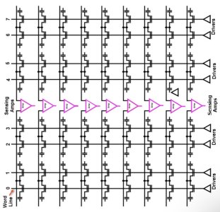
In a prior article I explained the difference between static and dynamic circuits. As I discussed there, dynamic circuits typically consume more power because they are constantly moving charge around, while static circuits only move charge when it is necessary to change logic value.In a DRAM memory, there are a collection of memory cells arranged in a grid.
Each memory cell has a capacitor, and at least one transistor. Wordlines run horizontally through the cells in a row, and are used to address the row. Addressing refers to the process by which you select which row is to be read from or written into. To choose the row, you set a voltage on the relevant wordline.
If you want to read, for example, a 32-bit word all at once, your memory would be 32 bits wide, meaning that each row would have 32 memory cells in it. The depth of the memory is how many rows the memory has.
It’s possible to design a DRAM so that you can read from or write to more than one row at a time, but for the sake of simplicity we’ll discuss a “single port” DRAM - that is, a DRAM where you read or write only row at a time.
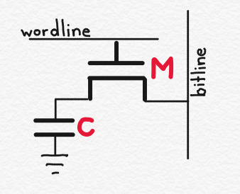
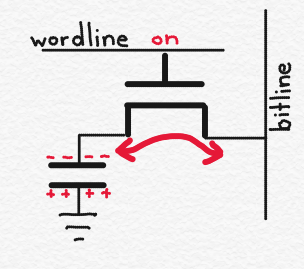
The above figure shows the circuit for a single memory bit cell. It consists of a capacitor, C, and a transistor, M. In Part 3 of this series, I discussed capacitors, and explained that a capacitor is a structure that stores electrical charge. I also discussed field effect transistors (FETs), and explained that depending on the voltage on the FET’s gate, charge may move through the transistor from its drain to source (or vice versa).
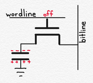
Let’s assume that the wordline is “off.” In other words, it is at 0 volts. This means that the transistor, M, is “off,” and no charge can flow across it. As a result, the electrical charge on the capacitor (shown with +’s and -‘s) is stuck on the capacitor. Let’s assume that if a memory bit cell‘s capacitor is charged then the memory cell is storing a logic 1, while if the memory bit cell’s capacitor is not charged then the memory cell is storing a logic 0. (This is arbitrary).
If, on the other hand, the wordline is “on,” say because its voltage is Vss (say 1 volt), then the transistor turns on, and electrical charge stored on the capacitor can flow through the transistor to the bitline. Putting charge on the bitline will affect its voltage, because voltage is equal to the charge on the bitline divided by the capacitance of the bit line.
So by monitoring the voltage on the bitline, I can determine whether or not the capacitor was charged prior to the wordline being asserted. In that way, you can read the memory. (Note that the change in voltage is very small, and there is generally an amplifier connected to each bitline to magnify the voltage change when the memory is read).
Charge can flow through the transistor in both directions. So if the goal is to write a logic 1 into the circuit, one can first put charge on the bitline (i.e. increase its voltage), then assert the relevant wordline. If the capacitor is not already charged, then it will become charged once the charge flows from the bitline to the capacitor.
Each DRAM memory cell is very small - it contains only a capacitor and a transistor. This allows very high memory density - you can fit a lot of memory into a small space.
There are disadvantages to DRAM, however. Let’s think about reading a DRAM cell, again. When you read a DRAM cell, the charge flows from the capacitor onto the bitline. But that means that there isn’t charge on the capacitor anymore. The DRAM cell held a logic value of 1, until I read the DRAM cell. The act of reading the DRAM cell removed the charge from the capacitor, so it no longer holds a value of 1.
When you read a DRAM cell, therefore, you generally need to write its contents back into it after you are done, otherwise it will no longer maintain its value. This takes power.
Secondly, as discussed in Part 3 of this series, transistors can “leak.” In other words, it is often difficult to turn a transistor all the way off. This means that, over time, charge from the capacitor can escape across the transistor and onto the bitline (or vice versa), potentially causing the memory cell to lose its value. Probably more importantly, the capacitor, itself, leaks. These capacitors are “MOS capacitors,” and are constructed similarly to MOSFETs. Due to the small dimensions, the capacitors do lose their charge over time (here, “over time” means something like 10s of milliseconds).
All of this means that even if not being read, the memory cells need to be periodically (many times per second) “refreshed.” This requires reading out the contents of the memory cells and writing them back again. This takes yet more power.
Finally, the semiconductor fabrication process used to make DRAM is optimized in a different manner than the semiconductor fabrication process used to make logic circuits, at least ideally. Logic wafers are optimized to make transistors that switch as quickly as possible. DRAM processes also use different mask steps to allow for vertical structures that don’t exist in logic wafers. For this reason, it is difficult to mix DRAM and logic on the same chip, or at least to do so in a way where the logic and memory are both optimized.
DRAM read access times vary, but 50-150ns is not unusual, though depending on how you measure, the number could be in the range of 10ns. Putting that in perspective, a CPU running at, say, 2GHz, has an access time of 0.5ns. This means that reading DRAM can take dozens, or even hundreds, of clock cycles, not even taking into account additional time to actually transmit the results from the DRAM to the CPU (which typically takes around 0.6ns per centimeter of distance). Putting this in perspective, if the CPU has to read data from off-chip DRAM, it may have to wait hundreds of clock cycles for the results. It is very unlikely that the CPU will be able to do other work during the entirety of this time. If an app is doing lots of memory accesses, and if doing so requires reading the results from off-chip DRAM, the CPU will likely spend a lot of time doing not much of anything, and performance of the CPU will slow to a crawl. (Consider this a preview of the next article, which will discuss caches).
In summary, DRAM tends to be power inefficient and slow, it usually can’t be integrated onto the same die as logic such as CPUs, but it does have the huge advantage of being able to squeeze a large amount of memory into a small space.
Static Memory
Another important type of memory is static memory (SRAM) [1]. Like dynamic memory, static memory is structured such that there is a grid of memory cells, each of which stores a single bit. Unlike dynamic RAM, however, static RAM does not use (much) power except when the data in the memory is changed. And static memory is typically built using the same semiconductor fabrication processes as digital logic, meaning it is easily incorporated onto the same die as the other logic in a CPU. Static memory structures are used in many places in a CPU. Probably the most important static memory structure in any CPU is the register file. (We’ll talk more about what the register file is used for in the next article in this series).Static memory structures are also used for things like TLBs, caches, branch prediction memories, and various other places depending on the microarchitecture.
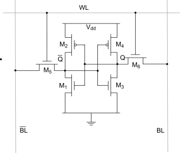
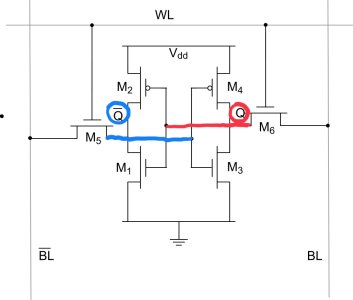
The figure above is a schematic for a typical SRAM memory cell, often called a “6T” cell because it contains 6 transistors. The “WL” wire at the top is the word line, which serves more or less the same purpose as the DRAM word line. On the left and right are two bitlines, labeled “BL” and “BL” with a line over it. In logic design, the line over a name indicates that it is the signal has the opposite value of the named wire. In other words, BL and BL with a line over it always have opposite logic values. (Sometimes we use an exclamation point instead of a line over the signal name, like BL!).
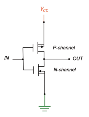
In a prior article, I discussed the static CMOS inverter cell. This is shown below.
If you look closely, you may notice that there are two inverters found within the 6T SRAM memory cell. One corresponds to the two transistors labeled M3 and M4. M4 is a p-channel FET (you can tell by the little circle, or bubble, on its gate). M3 is an n-channel FET.
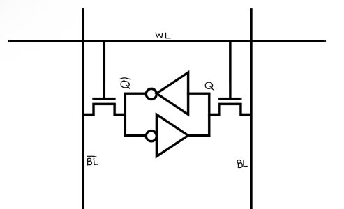
The second inverter corresponds to the two transistors labeled M1 and M2. We can therefore re-draw the circuit as follows:
The output of each inverter is connected to the input of the other. This is referred to as “cross-coupling.” Recall that the output of an inverter is always the opposite of its input. The logic symbol for an inverter is a triangle with a bubble on its output (or, if you want to be eccentric, on its input). The following figure is another way of illustrating cross-coupled inverters:

Imagine if the input into the first inverter is a logic 1. This is shown in blue on the left. This means the output of the second inverter has to be a logic 1. Because of the cross-coupling, this output feeds back into the original input all the way on the left. The values on the outputs of the inverters are thus self-reinforcing. A logic 1 on the input forces the input to be a logic 1.
And, as shown with the red values, a logic 0 on the input forces the input to be a logic 0.
This sort of self-reinforcing logic is very common in various kinds of memory structures.
Note that the output of the first inverter (the one on the left) has the opposite logic value from the output of the second inverter (the one on the right). These wires correspond to Q and Qbar in the circuit diagram for the 6T memory cell. I‘ve indicated Q and Qbar in red and blue below:
Typically, to read the value of the cell, you set the wordline to a non-zero voltage, and precharge the BL and BLbar wires. Transistors M5 and M6 are turned on, and current can flow through them. Depending on which of Q or Qbar is a logic 1 (one of them has to be and the other cannot be), current will flow through one of M5 or M6 (but not both). This will cause the voltage on either BL or BLbar to drop, which indicates the value that was stored in the memory cell.
To write a new value into the cell, you set and hold the voltage that you desire on each of BL and BLbar. You do this using strong enough drivers to overpower the inverters in the cell, so that even if the inverters are trying to produce one set of values, they are force to produce a different set of values. Since the bitlines are tied to the inverter inputs (through the ”pass transistors” M5 and M6), this has the effect of causing the inverters to start reinforcing the desired values, and setting the memory cell to the desired value.
SRAMs are bigger than DRAMs, for a given amount of memory. This is because each cell contains 6 transistors, including 2 PMOS transistors (which are bigger than NMOS transistors of equivalent strength). So SRAM is at a disadvantage when it comes to providing large amounts of memory.
On the other hand, SRAMs are much faster than DRAMs (usually). The precise speed depends on the design of the RAM and the process node, but a good rule of thumb is that you can read an SRAM in a tenth of the time of a DRAM (the advantage can be much more than that, depending on many factors). The power consumption of SRAM is also much less than DRAM. And SRAM can be easily integrated onto the same die as the other logic in a CPU, because the circuitry in the SRAM is very similar to regular logic circuitry.
Register Files and Caches, oh my…
All of the above is intended to provide the fundamentals for the next article, which will discuss caches. What I’ve tried to explain above is that we have two types of memory. Capacious but slow DRAM and fast but area-expensive SRAM. Long ago, computer architects discovered that you can combine the benefits of both of these types of memory in order to overcome the problems with each. The result is what we call caching.But even before there were caches, CPUs had register files. Register files are small static memories, usually, but not always, made up of 6T SRAM memory cells. (Early designs used other types of circuits such as “flip flops” or ”latches.”)
The idea behind register files is that, because it can take hundreds of clock cycles to read off-chip DRAM memory, it would be nice to keep some data in a small memory on the CPU chip, itself. The idea is that the register file can be read in a single cycle, so that, if the data needed by an instruction can be found in the register file, then there is no need for any delay to fetch the data; rather, the register file can be read as soon as the instruction is decoded, so that the data is ready as soon as the instruction is ready to be executed.
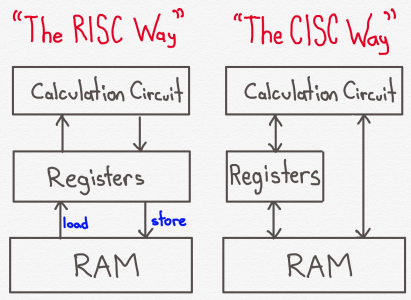
In RISC chips, there is a clear distinction between the use of registers and the use of external memory (DRAM). Typically, the only instructions that can access memory are
LOAD and STORE instructions. A LOAD instruction fetches data from memory and puts it in a register. A STORE instruction takes information from a register and puts it in memory. This is one of the primary ways to tell a RISC architecture from a CISC architecture; a RISC architecture typically only allows a very small number of instructions to access memory. In comparison, CISC architectures typically allow all sorts of instructions to access memory.So, for example, in RISC we may have something like:
In CISC, we may instead have something like:
Where the advantage of registers becomes helpful is where we are going to do many operations before needing to put the final answer back in memory. For example, in our RISC example, instead of storing R3 to memory we may first perform other mathematical operations on the contents of R3, like adding fees, rounding, etc. Each operation takes only one cycle, instead of the hundreds of cycles that each memory access may take.
Another characteristic of RISC architectures is that they tend to have more registers than CISC architectures. This is not a hard and fast rule, unlike the “RISC doesn’t allow tons of instructions to access memory” rule, but it’s a decent rule of thumb.
The idea of using a small register file that can be accessed in a single cycle to avoid having to perform memory accesses that take hundreds of cycles suggests what I will talk about next time - caches. If I can access a register file in one cycle, and memory in, say, 200 cycles, what would happen if I had some other memory that is bigger than a register file, smaller than the RAM memory, but takes, say 20 cycles to access? We call that “other memory“ a cache.
The principle is the same. The primary difference is that a register file is something that needs to be understood by software (at least by the compiler). The compiler determines which registers to use. If your new model of microprocessor adds registers, existing software can‘t make use of it. And if your new model of microprocessors removes registers, existing software will break.
By contrast, caches are designed (usually) to be transparent to software. Software is supposed to be able to run just fine regardless of whether there is a cache, and regardless of the cache’s size or other properties. Most of the complications of cache design are related to this need for the cache behavior to be transparent to the CPU. Which is a discussion for next time.
[1] While an “S” prefix often means “static,” SRAM should not be confused with another type of RAM called SDRAM. In SDRAM, the “S” stands for “synchronous.” In ordinary DRAM, once you select an address to read, the outputs will reflect the result at some point in time after the address is set. The time delay will depend simply on how long it takes for the read to take place. SDRAM is essentially DRAM except it behaves synchronously. “Synchronously” means that it works with a clock signal, so that the address doesn’t take effect until a clock signal arrives, and the result will be valid on some subsequent clock signal. Physically, SDRAM circuits are not very different from DRAM circuits; the differences aren’t in the memory bit cells, but are in the circuitry on the periphery of the memory block.

