I replied to the ATP mastodon account with some questions about their assertion and a link to a video by Ian Cutress. Here is the video
Ian surmises that DDR5 has ECC but really only for chip manufacturers to increase yields, not to protect user data.
John Siracusa tagged in Joe Lion, one of the people who wrote in and mentioned ECC on LPDDR5. It turns out Joe Lion is a chip engineer working for Micron! A product engineer according to his LinkedIn
https://www.linkedin.com/in/josephlion/
He was nice enough to reply to me with his thoughts and I will post them now. They are a series of “toots” from Mastodon. I will post both the links and the text. The starting point for the conversation was his thoughts on Ian's video:
"That video is true that on-die ECC has become, essentially, a “must” for advanced process nodes to get good enough yields to make DRAM continue to be economical. And, DDR5 has some “single bit forgiveness” built in, where customers KNOW that some small number bits on the DRAM may need to be corrected most of the time, even at time-zero. 1/3"
@jimmyjamesuk@mastodon.social @siracusa@mastodon.social That video is true that on-die ECC has become, essentially, a “must” for advanced process nodes to get good enough yields to make DRAM continue to be economical. And, DDR5 has some “single bit forgiveness” built in, where customers KNOW...

mstdn.social
"The DRAM monitors and reports (upon request) whenever it detects and fixes any errors. However, regardless of what the primary motivation for the on-die ECC is, the end result is that the data in the array IS more protected than it is in non-on-die chips. So, if you get a heat-induced cosmic-ray-induced bit flip on a regular DDR4 chip, you’re SOL. But if that happens on a DDR5 or LP4 or LP5 chip, then the on-die ECC will correct it for “free”. 2/3 (or 2/4, maybe?)"
@jimmyjamesuk@mastodon.social @siracusa@mastodon.social The DRAM monitors and reports (upon request) whenever it detects and fixes any errors. However, regardless of what the primary motivation for the on-die ECC is, the end result is that the data in the array IS more protected than it is in...
mstdn.social
"But, as John mentioned, a system shouldn’t truly say “we’re ECC protected” unless they also have system-level ECC, via ECC-based modules for DDR5 systems, or Link-ECC for LP5 SoCs. That’s why even with on-die ECC on all DDR5 chips, they still sell ECC-based RDIMM modules for servers. 3/4"
@jimmyjamesuk@mastodon.social @siracusa@mastodon.social But, as John mentioned, a system shouldn’t truly say “we’re ECC protected” unless they also have system-level ECC, via ECC-based modules for DDR5 systems, or Link-ECC for LP5 SoCs. That’s why even with on-die ECC on all DDR5 chips, they...
mstdn.social
"As to why Apple doesn’t advertise their ECC status? In my opinion, I think it’s an “out of sight, out of mind” issue for them. Now that they 100% control the entire CPU-to-DRAM data path by using SoCs (as opposed to allowing users to insert their own DIMMs), then basically I think they want to say “hey, don’t worry you’re pretty little heads about what goes on inside these chips. We’ll take care of that” 4/4"
@jimmyjamesuk@mastodon.social @siracusa@mastodon.social As to why Apple doesn’t advertise their ECC status? In my opinion, I think it’s an “out of sight, out of mind” issue for them. Now that they 100% control the entire CPU-to-DRAM data path by using SoCs (as opposed to allowing users to insert...
mstdn.social
"in traditional DDR4-style module based ECC, it’s up to the memory controller to track corrections. So it’s a feature of the chipset/CPU as to how it wants to track and report corrections. With on-die ECC, the DRAM chips themselves do keep track of error correction counts, and that data can be requested and reset by special commands by the memory controller. So I suppose a DDR5 mem controller could expose that data to the OS too. Up to the chipset at that point."
@jimmyjamesuk@mastodon.social @siracusa@mastodon.social in traditional DDR4-style module based ECC, it’s up to the memory controller to track corrections. So it’s a feature of the chipset/CPU as to how it wants to track and report corrections. With on-die ECC, the DRAM chips themselves do keep...
mstdn.social
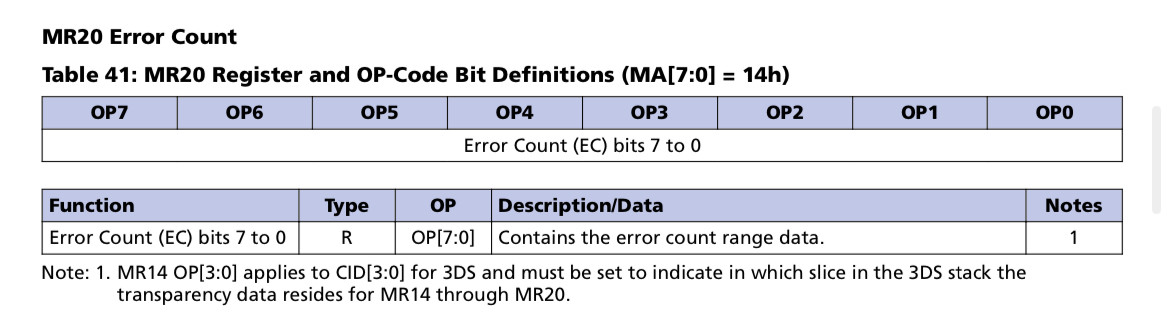
"here’s some excerpts from the standard DDR5 datasheet (the LPDDR5 datasheets are not publicly available) showing an internal Error Count “mode register” (that chipset can read) that I _think_ is incremented during regular error corrections, and a special command called “error scrub” which will do a full array read+correct+write+[report error count] upon request "
Attached: 2 images @jimmyjamesuk@mastodon.social @siracusa@mastodon.social here’s some excerpts from the standard DDR5 datasheet (the LPDDR5 datasheets are not publicly available) showing an internal Error Count “mode register” (that chipset can read) that I _think_ is incremented during...
mstdn.social
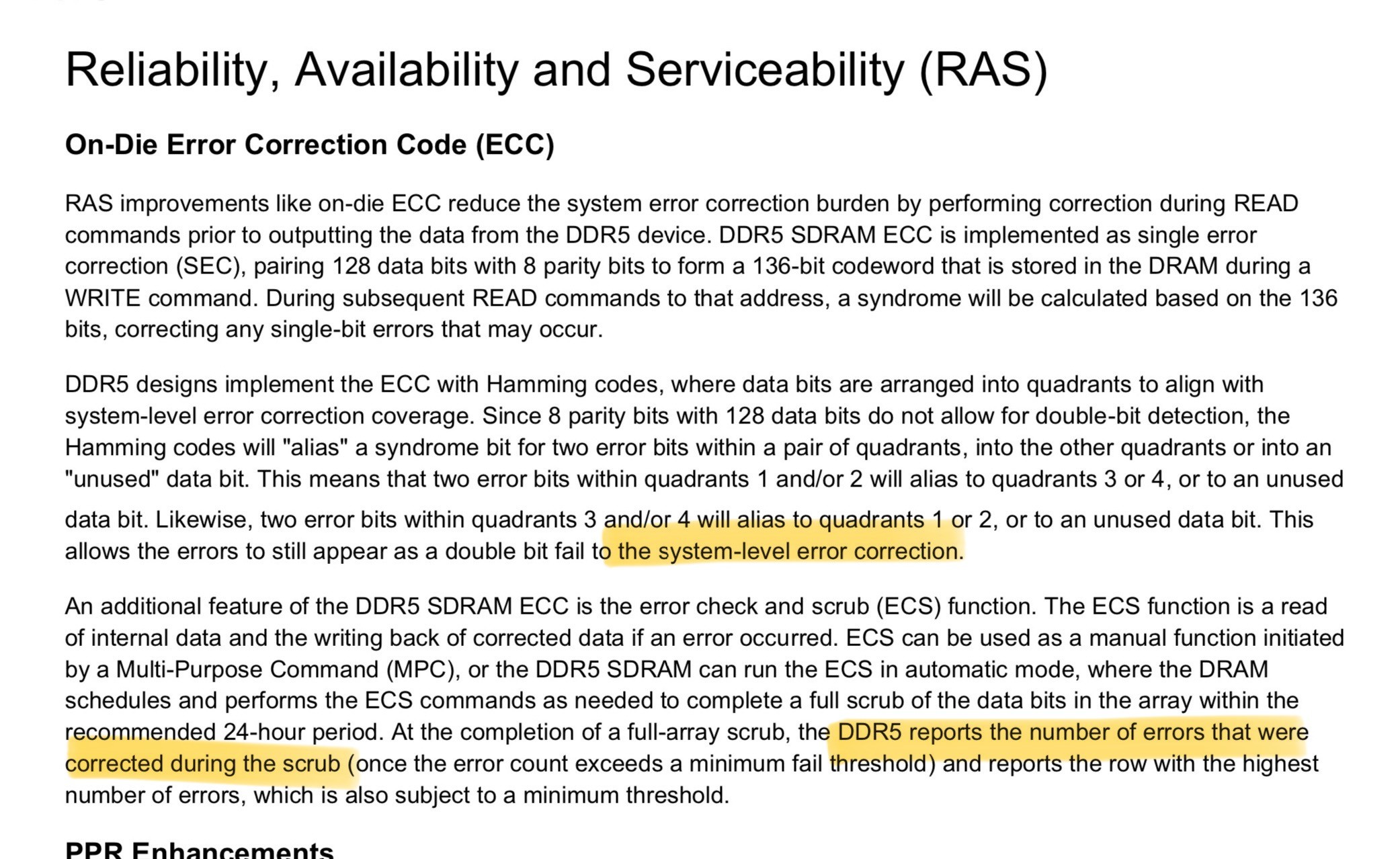
"also notice that even when announcing on-die ECC for DDR5, they still nod towards the need-for and existence-of system-ECC. Again, this is for DDR5. LP5 is similar, but LP5 specs are held much closer to the vest because of 1:1 relationships between memory suppliers and buyers. Unlike DDRx, which is often sold on open markets so all specs must be publicly available and fully standardized (or commodified)"
Attached: 1 image @jimmyjamesuk@mastodon.social @siracusa@mastodon.social also notice that even when announcing on-die ECC for DDR5, they still nod towards the need-for and existence-of system-ECC. Again, this is for DDR5. LP5 is similar, but LP5 specs are held much closer to the vest because...
mstdn.social
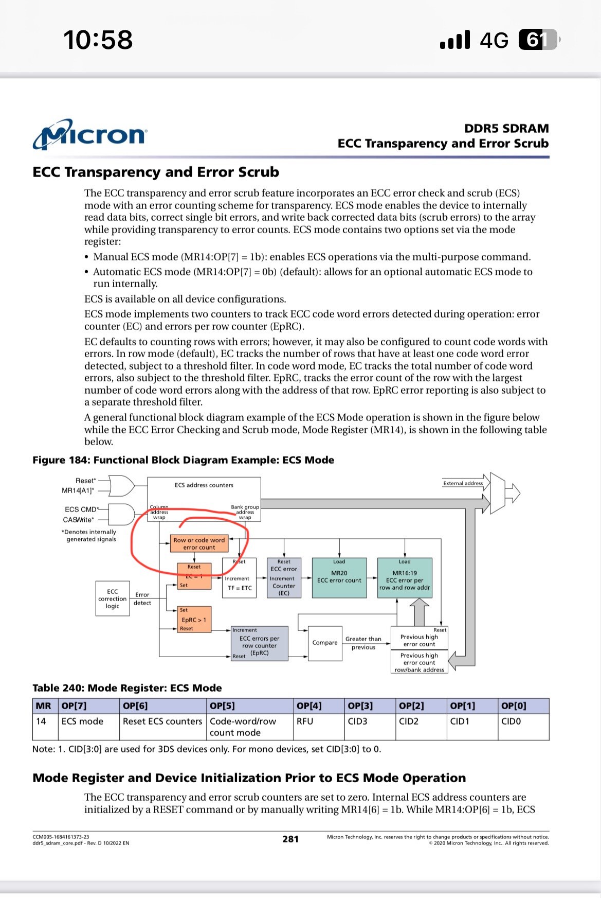
"damnit. Too many screenshots and links to manage on a phone. Meant to attach this overview of the Error Scrub command, which finds, fixes and counts error on demand"
Attached: 1 image @jimmyjamesuk@mastodon.social @siracusa@mastodon.social damnit. Too many screenshots and links to manage on a phone. Meant to attach this overview of the Error Scrub command, which finds, fixes and counts error on demand
mstdn.social
Following this exchange I asked if he thought On-Die ECC in addition to Link ECC and reporting of errors was equivalent to traditional ECC. His response was:
" I’m not a system engineer (I’m a chip engineer), but in my opinion, yes. LP5 on-die ECC + Link-ECC (if enabled) is functionally equivalent to server style module-based ECC. _Perhaps_ even better in real world usage, data can be corrected in 2 places? (bc we know data is clean when it leaves the DRAM, therefore allowing more correctable errors than before in transit. That depends on the specific correction capabilities) But I don’t know actual system-level results to back that up"
@jimmyjamesuk@mastodon.social I’m not a system engineer (I’m a chip engineer), but in my opinion, yes. LP5 on-die ECC + Link-ECC (if enabled) is functionally equivalent to server style module-based ECC. _Perhaps_ even better in real world usage, data can be corrected in 2 places? (bc we know...
mstdn.social
"following up on Apples motivations… Discussing ECC implies that errors are possible. IMO, Apple would prefer to not even mention it. Because, truth be told, the _vast_ majority of people would never even consider that. “The chips make mistakes? How? Why?” So why even bring it up? The small amount of nerds who are actually aware of ECC systems may wring their hands, but so what? 99% of people buying Macs and iOS devices just take it as read that the chips “just work”"
@jimmyjamesuk@mastodon.social @siracusa@mastodon.social following up on Apples motivations… Discussing ECC implies that errors are possible. IMO, Apple would prefer to not even mention it. Because, truth be told, the _vast_ majority of people would never even consider that. “The chips make...
mstdn.social
So after all that, it does seem like it is possible that ECC is implemented. It all depends on whether Apple is using Link ECC. To my knowledge, without someone on the inside saying, we can’t know.
Looking at
@leman patents, we can see some mentions of LPDDR5. The relevant parts I saw were:
"[0021] In some embodiments, the memory is an LPDDR5 memory that is configured to detect both link errors and on-chip errors. The memory controller may force a write link error correction code (ECC) error to maintain the poison status in this context."
"0054] The fifth generation of the Low-Power Double Data Rate (LPDDR) SDRAM technology was initially released in the first half of 2019. It succeeds its predecessor, LPDDR4/4X, and offers speeds of up to 6400 Mbps (1.5 times faster). Further, by implementing several power-saving advancements, LPDDR5 may provide a power reduction of up to 20% over previous generations. LPDDR5 may provide a link ECC scheme, a scalable clocking architecture, multiple frequencyset point (FSP’s), decision feedback equalization (DFE) to mitigate inter-symbol interference (ISI), write-X functionality, a flexible bank architecture, and inline on-chip ECC. LPDDR5 systems typically do not offer server-level reliability features such as single-device data correction (SDDC), memory mirroring and redundancy, demand scrubbing, patrol scrubbing, data poisoning, redundant links, clock and power monitoring/redundancy/failover, CE isolation, online sparing with automatic failover, double device data correction (DDDC), etc."
In conclusion, I don’t know.