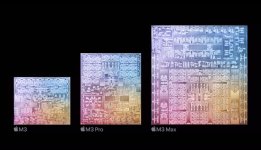
M3 core counts and performance

I guess what I’m asking is: Do the M3 GPUs even have fixed cache?

Well, it kind of has to, cache is a hardware structure that by definition has fixed limits. I think it’s better to think of it as fast on-core memory rather than traditional cache. The interesting thing about these GPUs is that when they run out of this internal fast memory they will fall back to using slower out-of-core memory to ensure consistent operation (normally GPUs will crash or refuse to start a program under these circumstances). In their tech notes Apple said the hardware is constantly monitoring the use of on-chip memory and will offload running tasks to ensure that data stays in the fast memory.
 
CUDA will
mirror data automatically, that’s how they achieve their coherency.

How automatic vs manual things are depends on the API, but for none of them does it mirror the data rather the newer APIs handle the automatic migration of it. CudaMallocManaged for instance migrates the data back and forth as needed though the programmer can supply hints as to when it would be optimal. The new thing is turn all regular memory allocations effectively into CudaMallocManaged. This is still in beta testing on Linux. An older API is used to explicitly pin Host (CPU) memory to reserve it for the GPU to communicate with and I still use it but I’m not sure that’s as necessary anymore. The most basic (or most advanced depending on your point of view) API is to manually manage data movement and explicitly allocate host (CPU) and device (GPU) memory. In all cases though it’s less about achieving coherence and more about ensuring that the data is always available where it needs to be. For CudaMallocManaged when the CPU has access to a piece of data, the GPU does not and visa versa. For manually managed data you can copy back and forth and simply not delete data from the source.

So @quarkysg is right that the most prominent use case is for when the working set is too large for the GPUs VRAM so you have to shuttle data in and out as it is being operated on. Program the migrations correctly and, depending on the workload, you can hide a lot of the latency … but you will still take a hit. You can’t hide all of it. Again this is where Apple’s UMA shines. Nvidia GPUs with lots of RAM are really really expensive.

However even with GPU centric calculations you do often also need to communicate intermediate and/or final calculations back and forth for the CPU, which is often still in charge of overall program execution, to decide what calculations to do next and/or what data to send next. That is another reason to copy data back and forth. It really all just depends on the program. But again with Apple’s UMA, there is less physical shuttling back and forth though the lack of a unified virtual table hurts here.
 
Last edited:
That depends on the API but it doesn’t mirror the data rather it handles the automatic migration of it. CudaMallocManaged for instance migrates the data back and forth as needed though the programmer can supply hints as to when it would be optimal.

Are you sure it works exactly like this, my understanding is that it copies the modified memory regions (on demand). It would be a waste to re-allocate and copy everything. Besides, CUDA ensures unified virtual address space, doesn’t it? It has to keep the addresses reserved on the CPU side (whether all pages are committed is another question of course).

In all cases though it’s less about achieving coherence and more about ensuring that the data is always available where it needs to be. When the CPU has access, the GPU does not and visa versa.

That’s exactly what I mean with coherence :)
 
Dynamic Caching is not about RAM at all. There is some confusion here because of the terminology used. When Apple says it helps with allocating memory, they are talking about GPU-internal memory, not the system LPDDR5.
Ah, right. I recall that now. But: Irrespective of the fact that Dynamic Caching doesn't address RAM, isn't over-reserving of GPU RAM a real thing? And if it is, and there's mirroring, would CPU RAM also be over-reserved (in systems with separate CPU and GPU RAM)? If it's not, then it seems having separate CPU and GPU RAM would "protect" the CPU RAM from this "overbooking".
In theory, but that’s not how it works in practice, as the data is usually mirrored in both memory pools. After all, GPU visible RAM on dGPU systems is limited, and you have to move things in and out to fit all your assets. CUDA will
mirror data automatically, that’s how they achieve their coherency.
I find coherency discomforting, as it runs counter to my normal incoherence.
 
Ah, right. I recall that now. But: Irrespective of the fact that Dynamic Caching doesn't address RAM, isn't over-reserving of GPU RAM a real thing? And if it is, and there's mirroring, would CPU RAM also be over-reserved (in systems with separate CPU and GPU RAM)? If it's not, then it seems having separate CPU and GPU RAM would "protect" the CPU RAM from this "overbooking".

I don’t quite follow. If memory is mirrored and you have overbooking, wouldn’t you have overbooking on both sides?

Talking about mirroring, I think it will depend on the driver and the application. OpenGL drivers did keep the full copy of data in the system RAM. Vulkan/DX implementations might behave differently. There is this promise of manual memory management in modern APIs, but how much of it is a driver imposed illusion I can’t say for certain.

And finally, the no-copy thing with UMA can be misleading as well. UMA systems don’t need a copy, but it doesn’t mean that copying is not happening. GPU APIs and applications are traditionally built around data copying, and Metal is no exception. A lot of this is build around the idea of ownership, and memory allocations used by the GPU are fundamentally owned by the driver. You do have APIs that allow you to use prior CPU-side memory allocations on the GPU, but there are limitations and they are not really drop-in. Maybe in a future Metal versions we will have the ability to use same data between CPU and GPU transparently. But we are still far off.
 
Are you sure it works exactly like this, my understanding is that it copies the modified memory regions (on demand). It would be a waste to re-allocate and copy everything. Besides, CUDA ensures unified virtual address space, doesn’t it? It has to keep the addresses reserved on the CPU side (whether all pages are committed is another question of course).


That’s exactly what I mean with coherence :)
Fair enough :) - and in fact the link below talks about this and coherence. And I was wrong you can get coherence (post-Pascal) if you make simultaneous calls from the GPU and CPU and the relevant data will exist on both sides (and be coherent right up until one of them makes a change) but in practice you basically never do that (that's a race condition most of the time). As a small practical point, I believe the memory addresses are actually kept on the GPU side. However, in terms of reserving memory and data locality that where things get interesting - basically it's up to the driver. When you initially call CudaMallocManaged, the driver may do nothing at all (at first)! It depends on what you do with the data next. Where you first "touch" the memory and populate it with data determines where the space for the data first exists and then you can create very complex access patterns for both sides, host and device. For some of these in theory you have to have at least some memory reserved on both system - however, how much *can* be dynamically changed over the course of the run. For instance let's say I have an 8GB GPU: if I create 10GB of Managed memory that I tell the driver should be created on the host first and populate it from the CPU, then the driver won't reserve the space on the GPU until the GPU calls for it or it gets prefetched and I can create as much GPU data as I want in the mean time. However, the moment I touch any part of that 10GB on the GPU, then yes space will be reserved on both but depending on what I do with the data the driver will make decision about how much GPU space to reserve and what to send over and may "free up" that space on the CPU depending on its choices. While it isn't it discussed in the link, in my admittedly poor memory of my testing this works the other way around as well - if I were to create 6GB of managed memory and tell the driver this is for the GPU and the first touch is on the GPU then the driver won't reserve host memory if I never touch it on the host. Yes giving that much control over to the driver can occasionally be inefficient and if the driver makes a bad call you end up having a page fault. So how much memory is reserved is a tricky question and mirroring where you have to have the full data reserved on both sides and existing on both sides simultaneously is basically not something that's done.

I want to stress you can almost always choose to manually manage everything and achieve the same results (an important exception later). In most cases, you don't have to use managed memory or make use of the unified virtual address space and in fact manually managing memory often yields faster performance and less wastage but results in a lot more coding with less flexibility. For managed memory you can choose to let the driver handle some of it for a small loss in performance but for critical sections turn some of your explicit memory management into hints for the driver. Truthfully for those sections you'll end up doing a similar amount of coding to the manually managed memory approach. Or for rapid prototyping or non-critical sections, you can just say I'll just allocate a bunch of managed memory (and soon all allocated memory will be managed - any regular new or malloc will count) and the driver will handle all of it for me and take the performance hit. Where the unified memory is truly necessary is if you don't know before you reach a piece of code which piece of memory you actually need to migrate, then page faults, up to the granularity of the page, gives you just the memory you need when you need it.


I don’t quite follow. If memory is mirrored and you have overbooking, wouldn’t you have overbooking on both sides?

I'm writing very slow I apologize, but as you can read above no. Data isn't mirrored by default in managed memory. It can be, but most often isn't. Managed memory is specifically designed to make overbooking GPU memory easy as opposed to having to manually transition data back and forth.

Talking about mirroring, I think it will depend on the driver and the application. OpenGL drivers did keep the full copy of data in the system RAM. Vulkan/DX implementations might behave differently. There is this promise of manual memory management in modern APIs, but how much of it is a driver imposed illusion I can’t say for certain.

And finally, the no-copy thing with UMA can be misleading as well. UMA systems don’t need a copy, but it doesn’t mean that copying is not happening. GPU APIs and applications are traditionally built around data copying, and Metal is no exception. A lot of this is build around the idea of ownership, and memory allocations used by the GPU are fundamentally owned by the driver. You do have APIs that allow you to use prior CPU-side memory allocations on the GPU, but there are limitations and they are not really drop-in. Maybe in a future Metal versions we will have the ability to use same data between CPU and GPU transparently. But we are still far off.

Yeah this is what boggles my mind. So you do still have to make copies at least some of the time. It seems to me that combining Apple's UMA and Nvidia's UVMA you could circumvent all of that. Maybe I'm wrong and there's a wrinkle I'm not getting, but it just seems so natural: no page migrations, no page faults, just one unified memory table with one physical memory location accessible by both the CPU and GPU (again, having to take care of race conditions of course). It seems like that should be very possible with Apple's hardware approach. It would simplify programming and make things faster and less wasteful. Of course if it were “easy” to do, then I’m sure they would’ve done it so there are probably complications that I’m not seeing.
 
Last edited:
Thanks to the memory values provided by @theorist9, I created a more complete overview of the different Mx chips.

1699896639282.png
 
Apologies if this has already been covered, but has anyone confirmed that the M3 Npu is the same as the A17, or is that still in doubt?
 
Apologies if this has already been covered, but has anyone confirmed that the M3 Npu is the same as the A17, or is that still in doubt?
I don’t think I’ve seen anyone cover it, but it would be extremely odd to have the A17 CPU and GPU but an earlier NPU. They’d have to do extra work to bring the older NPU forward. So it’s still a possibility but I would say very unlikely - more like just different marketing numbers making it seem like it’s an older NPU.
 
Apologies if this has already been covered, but has anyone confirmed that the M3 Npu is the same as the A17, or is that still in doubt?
But the A17 and M3 are on N3, which is a completely different process from N4/N5. They have to do the FinFlex layout for N3, so using an older NPU pattern with the newer process would just not make any sense.
 
Last edited:
Also, I'm pretty sure the M3 Max 16/40 does not have the UltraFusion connection at the bottom. Previous images of the Max dies that Apple released do not show a finished bottom edge, while all of the M3 Max edges look real.

So, I see two possibilities:

1) The Ultra will be based off of the M3 Max 14/30, with the UltraFusion connection replacing the 10 GPUs and 4 LPDDR5 blocks. The UltraFusion connection could be at the bottom only, or it could be part of the bottom and part of a side for a "pinwheel" arrangement with a small die in the center for routing. If they make both dual and quad die versions, the M3 lineup would be a pretty impressive: M3 8/10, M3 Pro 12/18, M3 Max 14/30, M3 Max 16/40, M3 Ultra 28/60, M3 Ultra 56/120.

2) The blank areas between the CPUs and GPUs on the M3 Max 16/40 hide through silicon vias for stacking dies. Thermals would be challenging, but, if anyone can do it, it'd be the engineers at Apple and TSMC.
 
all three are different
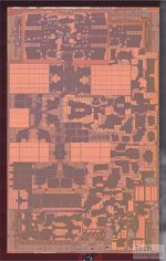
That is actually a pair of P-cores in each shot. And the exposure for the A17 is different enough that I would not claim with confidence that the A17 core is not exactly the same as the M3.
 
That is actually a pair of P-cores in each shot. And the exposure for the A17 is different enough that I would not claim with confidence that the A17 core is not exactly the same as the M3.
They are indeed pairs; it seemed a bit easier to see the differences that way. I should have mentioned that.

Anyway, the original A17 image is a bit clearer and I'm pretty certain that the P-cores are different. But don't take my word for it-- here are my source images!

Edit: the forum resized the images 😕
 

Attachments

Last edited:
I’m also downloading the iPhone 14 Pro and 15 Pro ipsws to analyze the ANE firmware. I really don’t think that anything in the M3 family is “based on” the A16 for a number of reasons, but I’m sick of all of the clickbait articles, videos, threads, etc., and it needs to be put to bed.
 
The A17/M3 family are "based on" A16/M2 in the sense that those were "based on" preceding architecture, back to A11 (the first 64-bit-only chip), all the way back to A7 (the first 64-bit chip). The processor architecture is improved in every iteration but it is unlikely that any generation is clean-sheet. The basic design principles are consistent. If "based on" is being used to mean they just carried the same tapeout forward, well, Cliff can tell you that is absurd.
 
The A17/M3 family are "based on" A16/M2 in the sense that those were "based on" preceding architecture, back to A11 (the first 64-bit-only chip), all the way back to A7 (the first 64-bit chip). The processor architecture is improved in every iteration but it is unlikely that any generation is clean-sheet. The basic design principles are consistent. If "based on" is being used to mean they just carried the same tapeout forward, well, Cliff can tell you that is absurd.
That’s why I put it in quotes, ya know, ‘cause I was quoting said clickbait crap. And I know that using the same design from a larger node is silly, hence the “number of reasons,” such as the images of those blocks on the dies are completely different. But there’s nothing preventing laying out the same logic on a new node, which I guess is what some people are yammering on about. If that were the case, I’d expect the firmware to be practically identical.

Edit: BTW, the M3 Pros and Maxes use the same firmware (but have different layouts), while the M3 uses different firmware. I haven’t had the chance to prise into them yet, however.
 
Last edited:
Anyway, the original A17 image is a bit clearer and I'm pretty certain that the P-cores are different. But don't take my word for it-- here are my source images!
For what it's worth, I wouldn't be super confident that these are actually different cores. The overall layout appears very similar, and you have to account for the way die shots are produced. When all the metal layers are intact, you can't see much at all as the last metal layers are power distribution - giant, featureless power planes that completely obscure everything behind them. Die shots are traditionally taken with a bunch of metal layers etched away. (Or never laid down in the first place - sometimes a wafer gets scrapped partway through the process and some of those get used for PR purposes.) The layers which are still present influence the shapes you see.
 
For what it's worth, I wouldn't be super confident that these are actually different cores. The overall layout appears very similar, and you have to account for the way die shots are produced. When all the metal layers are intact, you can't see much at all as the last metal layers are power distribution - giant, featureless power planes that completely obscure everything behind them. Die shots are traditionally taken with a bunch of metal layers etched away. (Or never laid down in the first place - sometimes a wafer gets scrapped partway through the process and some of those get used for PR purposes.) The layers which are still present influence the shapes you see.
For sure, though the A17 die shot is from Tech Insights, and they do really quality work. I also wouldn’t expect the same artifact on every P-core.

I’m also in the process of writing a script that finds all similar blocks and merges them with a multiple image super resolution algorithm. It’s turning out to be a fun little project.
 
Back
Top