I almost put this in @Cmaier ’s Don’t do that thread it never works thread, but I’m not actually sure if anyone has done this before.
 www.techpowerup.com
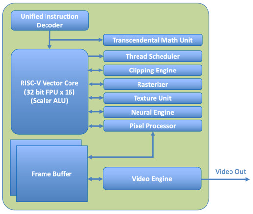
The CPU/GPU/NPU are not just on the same silicon sharing the same memory a la Apple Silicon but are the same processor, sharing the same instruction stream.
Honestly, this doesn’t sound great. But it certainly should be interesting if it ever sees the light of day. Which it probably won’t. What do y’all think? Innovative? Innovative trash? Or just trash?
X-Silicon Startup Wants to Combine RISC-V CPU, GPU, and NPU in a Single Processor
While we are all used to having a system with a CPU, GPU, and, recently, NPU—X-Silicon Inc. (XSi), a startup founded by former Silicon Valley veterans—has unveiled an interesting RISC-V processor that can simultaneously handle CPU, GPU, and NPU workloads in a chip. This innovative chip...
The CPU/GPU/NPU are not just on the same silicon sharing the same memory a la Apple Silicon but are the same processor, sharing the same instruction stream.
Honestly, this doesn’t sound great. But it certainly should be interesting if it ever sees the light of day. Which it probably won’t. What do y’all think? Innovative? Innovative trash? Or just trash?


 .
.