New “innovative” RISC-V chip with CPU/GPU/NPU combo processor

dada_dave

Elite Member
Joined
Oct 25, 2022
Posts
3,110
I almost put this in @Cmaier ’s Don’t do that thread it never works thread, but I’m not actually sure if anyone has done this before.
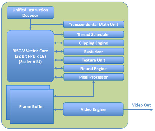

The CPU/GPU/NPU are not just on the same silicon sharing the same memory a la Apple Silicon but are the same processor, sharing the same instruction stream.

Honestly, this doesn’t sound great. But it certainly should be interesting if it ever sees the light of day. Which it probably won’t. What do y’all think? Innovative? Innovative trash? Or just trash?
I’m not sure what to make of it. It presumably has separate graphics execution units that can run in parallel with the ALUs. But sharing a single instruction stream seems like a bad idea (in terms of things like caching, branch prediction, etc.). But I don’t know much about graphics.
 
I’m not sure what to make of it. It presumably has separate graphics execution units that can run in parallel with the ALUs. But sharing a single instruction stream seems like a bad idea (in terms of things like caching, branch prediction, etc.). But I don’t know much about graphics.
I think it's using the vector processing units for the graphics so it has a single ALU and 16 FPU per vector core. And the whole thing is just these vector cores. Not sure how performant the CPU side will be with such a structure ... or any of it really.

EDIT: You know now that I think of it some more ... it kinda reminds me of Cell processors a little. They're not really the same design, but sorta similar in design intent. A little bit of Intel's Xeon Phi/A64FX too.
 
Last edited:
I think it's using the vector processing units for the graphics so it has a single ALU and 16 FPU per vector core. And the whole thing is just these vector cores. Not sure how performant the CPU side will be with such a structure ... or any of it really.

EDIT: You know now that I think of it some more ... it kinda reminds me of Cell processors a little. They're not really the same design, but sorta similar in design intent. A little bit of Intel's Xeon Phi/A64FX too.

I guess my concern is, in reality, if you are designing software that uses graphics hardware, how intermingled do the CPU and graphics instructions want to be? Your cache has only so much capacity, and you are now using a bunch of it for two things that seem somewhat unrelated to me (CPU instructions and graphics instructions). If you have a cache miss or a TLB miss or a branch miss prediction, now you are flushing in-flight graphics instructions too? I guess I just don’t know exactly what they have done here, or how well it maps to what software really wants to do.
 
I guess my concern is, in reality, if you are designing software that uses graphics hardware, how intermingled do the CPU and graphics instructions want to be? Your cache has only so much capacity, and you are now using a bunch of it for two things that seem somewhat unrelated to me (CPU instructions and graphics instructions). If you have a cache miss or a TLB miss or a branch miss prediction, now you are flushing in-flight graphics instructions too? I guess I just don’t know exactly what they have done here, or how well it maps to what software really wants to do.
According to the description each core can be independently assigned/programmed a function HPC, graphics, AI, etc ... so I would guess that an individual core wouldn't be doing multiple kinds of tasks and so sharing L1 might not be a problem? I dunno. Tom's talks about eDRAM/SRAM being used as L2 with no mention of what kind of L2 cache it would be nor is any kind of L3 mentioned.

I agree it all seems a touch odd - in addition to your objections, any vector core doing normal non-vector worlds is going to be very, very under utilized and integer performance is going to be disappointing even relative to standard GPUs which often have symmetric ALUs and FPUs in their compute cores. And on the flip side it's definitely the case that a lot of the silicon needed to build high performance CPU cores is often extraneous for GPU workloads. I was amused that Tom's was also reminded of Intel's Larrabee GPU, which is what become Xeon Phi which is also now defunct, as is Cell, so maybe moving this under the "this never works" thread is appropriate after all. Though hey I guess third time's the charm? Or is this fourth? You've got Larrabee and Xeon Phi (which is Larrabee 2.0 without the rendering) and Cell, but I'll admit A64FX is a bit of a stretch (and was far from a failure for its design goals). So two and half/three attempts so far.
Oh, that;s even more dubious. A core that is only being a GPU or only being a CPU at a given time is going to be designed in such a way that it is non-optimal for either purpose.
 
I think it's using the vector processing units for the graphics so it has a single ALU and 16 FPU per vector core. And the whole thing is just these vector cores. Not sure how performant the CPU side will be with such a structure ... or any of it really.

EDIT: You know now that I think of it some more ... it kinda reminds me of Cell processors a little. They're not really the same design, but sorta similar in design intent. A little bit of Intel's Xeon Phi/A64FX too.
Disagree on the Cell comparison, only because I agree completely on the Xeon Phi comparison. Phi AKA Larrabee tackled graphics by adding some texture sampling units to a chip that was otherwise a sea of x86 cores with 512-bit vector units, and this sounds a lot like that.

Cell didn't (iirc) have texture samplers or other graphics things coupled to its parallel CPU cores. What it did have was a stupid architectural choice which sabotaged the usefulness of its many cores in the real world: they thought it would be fine to skip building not just cache coherency, but any kind of shared memory at all. Only one core (the main PowerPC core) could access the main system memory (DRAM). The compute accelerator cores were stuck with access only to their own local scratchpad SRAM. The only communication between these memories (and therefore cores) was a programmable DMA copy engine, and maybe a mailbox register kind of scheme.

As I understand it, Sony did plan on doing graphics on the compute cores, but it proved to be too difficult and they were forced to throw a discrete GPU (sourced from Nvidia) into the PS3 late in the design cycle, causing huge delays. Intel did actually get graphics working on Larrabee, but cancelled it for mostly political reasons. Here's something Tom Forsyth (one of the graphics people who worked on the project) wrote up about it:

https://tomforsyth1000.github.io/blog.wiki.html#%5B%5BWhy%20didn't%20Larrabee%20fail%3F%5D%5D
 
Disagree on the Cell comparison, only because I agree completely on the Xeon Phi comparison. Phi AKA Larrabee tackled graphics by adding some texture sampling units to a chip that was otherwise a sea of x86 cores with 512-bit vector units, and this sounds a lot like that.

Cell didn't (iirc) have texture samplers or other graphics things coupled to its parallel CPU cores. What it did have was a stupid architectural choice which sabotaged the usefulness of its many cores in the real world: they thought it would be fine to skip building not just cache coherency, but any kind of shared memory at all. Only one core (the main PowerPC core) could access the main system memory (DRAM). The compute accelerator cores were stuck with access only to their own local scratchpad SRAM. The only communication between these memories (and therefore cores) was a programmable DMA copy engine, and maybe a mailbox register kind of scheme.

As I understand it, Sony did plan on doing graphics on the compute cores, but it proved to be too difficult and they were forced to throw a discrete GPU (sourced from Nvidia) into the PS3 late in the design cycle, causing huge delays.
Aye that’s what I was going for that Cell was designed as a GPU-like CPU but also had some “interesting” design decisions. I didn’t realize that they’d also tried to run graphics on it at one point but that makes sense. But yeah the actual design was pretty different even though the overall goal was the same/similar.

Intel did actually get graphics working on Larrabee, but cancelled it for mostly political reasons. Here's something Tom Forsyth (one of the graphics people who worked on the project) wrote up about it:

https://tomforsyth1000.github.io/blog.wiki.html#%5B%5BWhy%20didn't%20Larrabee%20fail%3F%5D%5D

Very informative post, thanks! I’ve definitely heard of Tom, didn’t know he was involved with Larrabee. Intel’s Xeon Phi always struck me as a neat idea but ultimately clunky. Naturally as part of the design team he feels the opposite way about it, that the approach is superior to GPGPU, but a lot of the things he lauds in the piece such as no scratchpads, TSO, legacy compatibility, emulating graphics in software, etc … seems like missing functionality or unnecessary overhead to me. But then I come from the GPGPU perspective so that could be my bias.

Also it’s hard not to see with the benefit of 7+ years of hindsight that AVX512 is currently in a more difficult position in the market than I think Intel had predicted - though as is common on x86 these days, AMD seems to have more successful designs with it than Intel itself. So that may be unfair to AVX512 as part of the issue is that it doesn’t gel with Intel’s hybrid core processors and Intel just runs too hot overall.

I think that post is also being a little too kind to that era’s “Gen” GPUs. While Intel is making progress, given the struggles Intel has had scaling up their designs, drivers, etc … all these years later and how much further behind they were then, it’s pretty clear that back in 2016 that they wouldn’t just (easily) “build a great one [big hot discrete GPU]” with their “Gen” designs.

Despite what I wrote above I do wonder though what the team might’ve achieved had they continued to iterate on their design. I know that there were definitely some people who were very excited about the approach to parallel computing.
 
Very informative post, thanks! I’ve definitely heard of Tom, didn’t know he was involved with Larrabee. Intel’s Xeon Phi always struck me as a neat idea but ultimately clunky. Naturally as part of the design team he feels the opposite way about it, that the approach is superior to GPGPU, but a lot of the things he lauds in the piece such as no scratchpads, TSO, legacy compatibility, emulating graphics in software, etc … seems like missing functionality or unnecessary overhead to me. But then I come from the GPGPU perspective so that could be my bias.
Yeah, he's definitely got rose-tinted glasses on. Also more defensible at the time he wrote it, IMO.

I see Xeon Phi as something that was compromised a lot by Intel management's dedication to two things: not spending much on it, and x86 everywhere. Why else would you start by modifying a plain Pentium core? Why use x86 at all in a chip with 40+ cores, given that the main market (HPC) and the secondary market (graphics) don't give a rip about x86 compat? The area and power overhead of x86 really starts to bite hard when you're trying to pack a chip full of these cores, I feel the only way they made it somewhat acceptable was to make the cores as small as possible relative to the giant vector execution units.

Also it’s hard not to see with the benefit of 7+ years of hindsight that AVX512 is currently in a more difficult position in the market than I think Intel had predicted - though as is common on x86 these days, AMD seems to have more successful designs with it than Intel itself. So that may be unfair to AVX512 as part of the issue is that it doesn’t gel with Intel’s hybrid core processors and Intel just runs too hot overall.
Yeah, Intel shot themselves in the foot a lot on AVX512. Kind of a perfect storm with their problems moving on from 14nm. They used to have a CPU design process that was tightly linked to the idea that they could roll out a new manufacturing node every two years without fail, and that assumption began to not hold around when they were due to roll out AVX512 across the whole line, so they got a little stuck (at least on the consumer side of things). Didn't help that they also kept wanting to treat AVX512 as an upsell feature, always the wrong thing to do with an ISA extension you want to be widely adopted by software.

I think that post is also being a little too kind to that era’s “Gen” GPUs. While Intel is making progress, given the struggles Intel has had scaling up their designs, drivers, etc … all these years later and how much further behind they were then, it’s pretty clear that back in 2016 that they wouldn’t just (easily) “build a great one [big hot discrete GPU]” with their “Gen” designs.
I think he's accurate with respect to hardware - by all accounts, Intel Arc GPUs seem to be fine on that front. What's let them down is that competitive Windows gaming performance requires an insane amount of per-game optimizations, due to an unhealthy ecosystem where it's routine for NVidia and AMD to fix game performance problems (or sometimes even correctness problems!) in their drivers. Turns out it takes a lot of time to go through the back catalog of games and develop decades worth of game-specific tweaks.

Supposedly Intel does very well on modern games that use modern APIs like Vulkan or D3D12, where there's much less scope for driver tweaks to affect things one way or another.
 
One way I could see mixing instruction streams would be to have a branch-and-execute instruction that tells the processor that the code immediately following the branch is for the alternate encoding and should be run by the device that is identified in the code block header, while CPU execution should resume at the branch target location. If the alternate code does not generate CPU dependencies or such that could be deferred to a later section of CPU code, such a scheme just might be practical. But, you have to have branching range adequate to handle interleaved blocks of alternate code, which might be non-small.
 
A new pizza ordering startup for y'all:


“Flow intends to lead the SuperCPU revolution through its radical new Parallel Performance Unit (PPU) architecture, enabling up to 100X the performance of any CPU,” boldly claimed the Flow CEO.

Sounds great!

Another eyebrow-raising claim is that an integrated PPU can enable its astonishing 100x performance uplift “regardless of architecture and with full backward software compatibility.” Well-known CPU architectures/designs such as X86, Apple M-Series, Exynos, Arm, and RISC-V are name-checked. The company claims that despite the touted broad compatibility and boosting of existing parallel functionality in all existing software, there will still be worthwhile benefits gleaned from software recompilation for the PPU. In fact, recompilation will be necessary to reach the headlining 100X performance improvements. The company says existing code will run up to 2x faster, though.
Impressive
PC DIYers have traditionally balanced systems to their preferences by choosing and budgeting between CPU and GPU. However, the startup claims Flow “eliminates the need for expensive GPU acceleration of CPU instructions in performant applications.” Meanwhile, any existing co-processors like Matrix units, Vector units, NPUs, or indeed GPUs will benefit from a “far-more-capable CPU,” asserts the startup.
Flow explains the key differences between its PPU and a modern GPU in a FAQ document. “PPU is optimized for parallel processing, while the GPU is optimized for graphics processing,” contrasts the startup. “PPU is more closely integrated with the CPU, and you could think of it as a kind of a co-processor, whereas the GPU is an independent unit that is much more loosely connected to the CPU.” It also highlights the importance of the PPU not requiring a separate kernel and its variable parallelism width.

This is starting to sound familiar which is why I posted it here. 🙃

For now, we are taking the above statements with bucketloads of salt. The claims about 100x performance and ease/transparency of adding a PPU seem particularly bold.

Oh really? Huh.

Another article:


Website:


Who knows right? One can get so jaded that you'll cynically respond to a real advancement but extraordinary claims require extraordinary evidence.
 
A new pizza ordering startup for y'all:


Sounds great!


Impressive


This is starting to sound familiar which is why I posted it here. 🙃


Oh really? Huh.

Another article:


Website:


Who knows right? One can get so jaded that you'll cynically respond to a real advancement but extraordinary claims require extraordinary evidence.
I read a couple articles and for the life of me can’t figure out what they’re on about.
 
I read a couple articles and for the life of me can’t figure out what they’re on about.
I'm not sure either. I was kind a hoping you or someone might clarify. The best I can make out from all the marketing is that it sounds like a somewhat more versatile/compute oriented GPU core that sits more closely to the CPU a la the AMX accelerator but has its own incredible fabric to the RAM that is super high bandwidth and doesn't need caches because it's so great. So anything multithreaded (like pThreads or GCD) can be shunted to this accelerator like the CPU already does for SME/SSVE2 but again this time it's *anything* multithreaded. And the accelerator can have any number of any kind of functional units to do any workload the designer wants and it has a superior method of connecting said functional units compared to current GPUs and CPUs.

I mean, I ain't a Computer Engineer but it sounds a bit like magic to me.
 
Back
Top