Tick tock.
To a CPU designer, a clock is a signal that is used to synchronize the behavior of different circuits. As discussed in earlier articles in this series, a CPU consists of two types of logic: synchronous logic and combinatorial logic. The synchronous logic consists of circuits that save state information - in other words, these circuits hold their value until a synchronization signal - a clock - comes along and instructs them to update their values. In other words, these are memories.
The combinatorial logic takes the output of the memory elements as its input, performs logical operations on it, and outputs the results to other memories which will capture them when the sychronization signal - the clock - tells them to.

The various synchronous circuits may all be synchronized using the same clock, different clocks, or different phases of the same clock. (I’ll discuss phases below).
But what, specifically, does this synchronization signal look like? “Time” for some nomenclature.

Above I‘ve drawn a “timing diagram” for a traditional, single phase, half duty cycle clock signal (don’t worry, I’ll explain those terms). The x-axis in this diagram is time. The y-axis is voltage. As you move from the left to the right, you are seeing how the voltage of the clock signal varies as time elapses. As drawn here, the voltage starts at 0 at time 0, and immediately rises (at time 0) to a high value. After some period of time, the voltage then falls back to 0, where it remains for some amount of time. This oscillatory behavior - rising and falling - is necessary for any clock signal.
A “period” of the clock is the time it takes for the clock to make one complete oscillation (“cycle”) - from 0 to high and back to 0 (or vice versa). I’ve indicated one period of the clock in red in the above diagram. The clock frequency - the number of cycles per second - is the multiplicative inverse of the period: 1 / period.
We talk about the clock “being high” or ”being low,” which refers to the relative state of its voltage at any given time. For our purposes, we seldom need to think about the actual values of these voltages, and it is sufficient to just know whether the clock is at (or near) its lowest or highest voltage. We sometimes refer to this as the “level” of the clock - in other words, is the clock currently at its high ”level” or low “level.”
I’ve also indicated a rising edge and a falling edge of the clock. A clock “edge“ occurs when the clock transitions from one level to another. The concept of edges is important, as I’ll discuss more below, but the basic issue is that circuits that respond to the clock sometimes only care about the level of the clock, but more often, at least in modern CPUs, care about the edges of the clock.
I talked about ”duty cycles” above and promised I would explain, and I keep my promises. The duty cycle of a clock signal is simply the percentage of the time that the clock signal is at its high level. In the timing diagram above, the duty cycle is simply 50%. It spends half its time high, and half its time low. But it doesn’t necessarily have to be that way. For example, here are a couple of clock signals that have 75% and 25% (or as close as my freehand drawings permit) duty cycles:

 Typically, for single phase clocks, the duty cycle is 50%, or as close to 50% as your circuit design skills permit. But I also promised I’d explain what a “phase” is. The above clocks are all presumed to be generated by some clock source somewhere, and transmitted by wires to synchronous elements scattered about the chip. I can take a look at any clock wire on the chip and know whether the clock is high or low, and “high” and “low” are the only two possible values for “clock” on my chip. Since only one clock wire is necessary in order to know everything there is to know about the clock, the clock is “single phase.”
However, more complicated systems are possible. In fact, the Exponential x704 I helped design used a “four phase” clock.

Here we learn that the greek Phi symbol is a nice shorthand for “phase,” and that CPU designers number everything starting at 0 (except for IBM, and who the heck can account for their taste).
Here we can imagine four different clock wires, each representing a single phase of the clock. In this case, only one clock is high at any given time. When that happens, that phase is said to be active. So, for example, I could have one memory element clocked by phase 0 that drives into some logic that produces a result which is captured by a memory element clocked by phase 2. Or, if the logic is more complex and I need more time, I can capture the result with a memory element clocked by phase 3. This is because the time difference between the assertion of phase 0 and phase 3 is longer than the difference between phase 0 and phase 2.

Note that here the pulses don’t overlap in time; only one phase is asserted at a time. This need not be the case. Overlapping clock phases are perfectly acceptable.
So far I’ve drawn the clock timing diagrams as lovely little perfect(ish) straight lines. But the actual clock waveform doesn’t really look like that. For example, because it’s impossible to make the voltages jump instantaneously from low to high, and because there is resistance and capacitance on the clock wires, the clock waveforms really look more like this:

And while I may think that my clock will be highly accurate, with each pulse having the intended width and the period staying the same between successive oscillations (or “cycles”) of the clock, that’s not likely to be the case. In reality, for example, you are likely to have at least some clock “jitter.”
 In the above diagram I’ve shown the expected, idealized, clock waveform in a thin gray line, and the actual clock waveform as a thick blue line. This imperfection, or jitter, occurs when the period of each cycle is not identical.
The clock is usually generated by a “phase-locked loop” (PLL). The PLL receives a reference clock, for example generated by an off-chip crystal. I’ve called this Fref in the figure below.

A voltage-controlled oscillator (VCO) on the chip creates another oscillating clock signal. Circuitry including a phase detector and a low pass filter is used to line up the VCO signal with the reference signal, to ensure that the on-chip clock has a reliable cadence. The use of a divider in the feedback loop allows the on-chip clock frequency to be a multiple of the reference clock frequency, and ensures that the on-chip clock edges line up with the reference clock edges (which can be helpful when multiple chips need to synchronize their clocks).
Note that when I refer to a “phase detector,” I am referring to a detector that detects the relative offset of two clock waveforms, which is slightly different usage than the prior discussion of clock “phases.” For example, the phase difference between two clock waveforms is indicated below.

I’ll talk some more about PLLs later, because they can be very useful for dealing with something called “clock skew.”
The clock gets distributed around the chip, to each memory element that it connects to, using what we call a “clock tree.” The clock tree starts at the clock generator (the PLL) and distributes the clock across the trip using wires and buffers.

Ideally, the buffers and wires are arranged in such a way that all of the memory elements receive the clock signals simultaneously. If they don’t, that’s called “clock skew,” which can be a major problem. To accomplish the clock distribution, buffers drive other buffers, and so on, until the clock signal arrives at each memory element (indicated in black in the figure above).

Let’s consider the two branches of the clock tree shown above in blue and green. Assume that the path to A takes 1 nanoseconds and the path to B takes 1.2 nanoseconds. Assume, too, that A is used as the input to some logic that produces an output that is supposed to be captured by B. And let’s assume that the clock cycle - the time it takes for a complete clock oscillation - is 2 nanoseconds. The following figure illustrates this:

Instead of 2 nanoseconds, the combinatorial logic can take 2.2 nanoseconds. This is because the clock always arrives at the right-side synchronous circuit 0.2 nanoseconds later than it does at the left-side synchronous circuit. In other words, at time zero, the left-side clock arrives and the combinatorial logic receives its inputs. It needs to produce its outputs before the right-side clock arrives. This will happen 0.2 nanoseconds (200 picoseconds) later than it would have if there were no clock skew.
If that’s all there was to it, this would be great news. In fact, when I took over the integer execution unit on AMD’s K6-II, I routinely took advantage of this effect, which we called “clock borrowing,” to enable us to speed up the chip’s clock; if I couldn’t find a way to shave the necessary 100 picoseconds off of some timing path in the adder, but the downstream path’s all had 100ps to spare, I would purposely slow down a clock so that the critical path had 100 extra picoseconds and the next stage of paths had 100 fewer. We were wild and crazy back then, and this is not a great idea for a bunch of reasons. Perhaps that’s for a later article.
In any event, clock skew is not always ”good.” Let’s consider this same situation, with just a touch more detail.

Here I’ve shown two of the many paths through the combinatorial logic - a fast path and a slow path. The slow path takes 500ps to change its output once its inputs change. The fast path takes only 100ps. Let’s look at a timing diagram representing all of that:
 The way the circuit is meant to work is that when the rising edge of the clock arrives at A, a new set of inputs is provided to the combinatorial logic. In our timing diagram that happens when time = 0. The combinatorial logic does its thing, and produces its results by the time the rising edge of the clock arrives at B. If there were no clock skew, then the first rising clock edge after time 0 would occur at time 2000 (because the cycle time is 2 nanoseconds).
Since both the slow path and the fast path need no more than 500ps to finish, they would calculate their new results in plenty of time.
But we have clock skew, which means that the clock at B is delayed by 200 ps as compared to the clock as A. This is shown on the timing diagram above.
The slow path, taking 500ps, produces new results after the first rising clock edge at B (indicated by the star), so that raising edge doesn’t capture anything new - it will capture the results of the previous cycle, which is what we want. But the fast path changes its output at 100ps, which means the new results will be captured at B when it receives a rising clock edge at 200ps. But that’s wrong. That raising edge is supposed to capture the prior cycle’s result. We sometimes call this a hold time violation.
The circuit is broken. Bad circuit. Clock skew did a bad thing.
Also, consider what happens if we reverse things, so that the clock takes 1200 picoseconds to arrive at A but 1000 picoseconds to arrive at B. Now, instead of having 2 nanoseconds for our timing paths, we have only 1800 picoseconds. If our combinatorial logic takes 2 ns, then it will not compute its results in time to be captured at B. And our circuit is broken again, this time due a setup time violation.
As a general rule, we try to minimize clock skew. And we model it - during the design process we calculate the delay of the clock to each memory element, and account for it to make sure we don’t have any setup or hold time violations.
There are many ways to arrange the clock’s metal wires on the chip, including grids, H-trees, and various hybrid approaches. One or more clock grids is very common. In a clock grid, large driver circuits distributed around the chip drive the clock signal onto one or more large metal grids. The metal grid will typically involve several metal layers. In a chip, the metal layer closest to the silicon is called M0 or M1, and each successively higher layer of the metal stack is given an incremented number. The wires on higher metal layers are wider, reducing their electrical resistance, and they are often used for long-distance wires and metal grids.

Above is an example of a clock grid. There may be multiple such grids on a given chip. The wires in the metal grid are driven with a lot of current. The grid is big, driving lots and lots of circuits, each of which has an input capacitance that requires charging and discharging quickly in order to produce nice, sharp, clock waveforms. This requires a lot of current.
If signal wires - the wires that connect the various logic gates - happen to run alongside the clock grid wires for long distances, this can cause a lot of noise to be injected into the signal wire, causing circuit malfunctions. In an earlier article, I discussed capacitance between wires, and explained how the parasitic capacitances between the wires is a function of the space between them, their cross-sections, and the material between them. And the “effective” capacitance between the wires can be higher than that. In 1996 I wrote an article, published in the IEEE Journal for Solid State Circuits, that explained that the effective capacitance is a function of the ratio of the edge rates between the two wires.

As shown in this figure, two wires may have different rise and fall times. In other words, as shown in the image above, the wire switching from low to high switches much faster than the wire switching from high to low.
In the paper I authored for Exponential Technology, we derived a figure we called “effective capacitance“ that is a function of the ratio, N, of these switching times. In other words, if two wires are next to each other and switch equally fast in opposite directions, N is 1. If one switches 10x as fast as the other, N is 10.

It turns out, the effective capacitance rises linearly until N=2. The maximum value is 3C, meaning that the effective capacitance can be as high as three times the physical capacitance. As a result, if a signal wire is, say, trying to transition from a 0 to a 1 and is doing so fairly slowly while running alongside a clock grid wire, the transition is likely to be either greatly delayed, greatly sped up, or flipped back and forth improperly in mid-transition. In discussing clock skew, above, I explained why a signal changing too quickly can cause a hold time violation and a signal changing too slowly can cause a setup time violation, both of which can break the operation of the processor. Clock skew isn’t the only cause of these sorts of issues - capacitive coupling can cause these problems too.
As a result, it’s not uncommon to shield the clock wires by surrounding them with power and ground wires.
 The above drawing illustrates such shielding. The green data wire is prevented from coupling to the clock wire by placing VSS (ground) on one side of the clock. VDD (the power line) is located on the other side of the clock. No wire can run directly next to the clock wire because of this.
Other tricks are sometimes used as well. For example, on one chip we routed the clock wire ”off the routing grid” so that there would (almost) always be extra spacing between the clock wire and data signals; we were taking advantage of the behavior of the signal routing software that we were using, whereby it preferred, when possible, to stay on a “routing grid.” The router will also try to avoid violating the process design rules, for example by purposely avoiding putting two parallel wires too close together.

The above figure shows the routing grid (in black). A wide, blue clock wire is placed (by “hand” - or, more likely, in-house CAD tools) between two routing grid lines. The red signal wires, automatically placed by the routing software, cannot be placed on the two routing tracks closest to the blue clock wire, because that would violate the minimum spacing design rule. So the router puts them on the next closest tracks. This means the spacing is a little further from the blue wire to the red wires than it would be if the blue wire was routed on a legal routing grid track.
Other tricks that I have seen include using ”blockages” that prevent the router from getting too close. For example, the clock grid can be presented to the routing software as being outrageously wide. The router software won’t intentionally short circuit a signal wire to the wide clock wires. After the routing software is done, in-house CAD software can post-process the results and replace the super-wide clock wires with smaller ones.
Another relevant sub-topic is clock gaters.

No, not clock gators.
In the prior article in this series where I discussed power consumption, I explained why the switching of signals cause power consumption. An important way to prevent unnecessary power consumption is to prevent memory elements from switching their outputs when their outputs aren’t needed. Clock gating is a design feature where you simply add a logic gate nearby the memory elements. The logic gate accepts the clock as one input, and a “clock enable” (or ”clock disable”) signal as another element. When the memory element is storing a value that is only useful for circuitry that is not needed in a particular clock cycle, you set the enable/disable signal appropriately.
You can either use a separate logic gate or build the enable functionality into the memory itself. The former has the advantage of taking less area and potentially less power consumption if you are controlling multiple memory elements with the same clock gater. If you are not doing so, however, it can be advantageous to build the gating circuitry into the memory element, itself.
Finally, I mentioned that the state elements (memory circuits) can be responsive to the level of the clock or to the edge of the clock. Everyone loves circuit diagrams, so here we go…
First, let’s talk about transmission gates. Transmission gates are tiny little circuits that pass current from one end to the other, or prevent current from passing, depending on an input. This is similar to the way a single transistor works, and sometimes you could just use a single transistor instead, but for the circuits we are talking about it is better to use transmission gates.

On the left, we see a transmission gate. A transmission gate is two transistors wired so that their sources are connected and their drains are connected. One is a PFET and one is an NFET. As we discussed in an earlier article in this series, an NFET is “on” when its gate is at a high voltage, and off when its gate is at a low voltage. A PFET, on the other hand, is on when its gate is at a low voltage and is off when its gate is at a high voltage.
If, as shown here, we connect the two gates to opposite polarities of the same signal - here Clock and !Clock - then both transistors will be on or both will be off. In other words, if Clock is at a high voltage, then, by definition, Clock! is at a low voltage (and vice versa).
As shown in the middle figure above, if we set Clock to a high value (logic 1), then the NFET will be on, and so will the PFET. This allows current to flow from one end of the transmission gate to the other.
And, as shown in the right figure above, if we set Clock to a low value (logic 0), then both the NFET and the PFET will be off, and no current can flow across the transmission gate.
The reason we sometimes use transmission gates instead of just using a single NFET or PFET (we call a single device wired that way a “pass transistor”) is that a transmission gate ensures that the voltage on each side of the gate is the same. If we were to use just an NFET, and assuming the left side is at a high voltage, when the NFET is turned on, the voltage on the left side will be a tiny bit higher than the voltage on the other side. In other words, a single NFET transistor (i.e. half a transmission gate) has difficulty passing a 1 accross itself; it passes what we refer to, sometimes, as a “weak 1.” PFETs, on the other hand, pass weak 0’s. Using both a PFET and an NFET ensures that the voltage is always what it should be, making the circui more immune to noise from external sources.
Now that all that is out of the way, let’s talk about latches. Latches are memory elements that are sensitive to the level of the clock. As long as the clock is a 1, for example, the input is passed to the output of the latch. And as long as the clock is a 0, the input is ignored and the output maintains its pre-existing value.
Below is a very simple latch design, and a design I’ve actually used many times.

You should recognize the presence of not one, but two transmission gates, as well as two inverters. Let’s look at what happens when the clock signal (CLK) is high.

When CLK is high, the left-most transmission gate is turned on, and current can flow through it. So I’ve replaced it with just a wire in the above figure. The other transmission is turned off, so it’s as if there is an open circuit there. For that reason, I’ve simply removed it from the above figure. The net result is a very simple circuit. The input signal, In, passes through an inverter, where it produces In! (the opposite of In) at the output of the circuit. The bottom inverter serves no purpose when the CLK is high, so we can ignore it (it produces an output that doesn’t go anywhere).
So, essentially, as long as CLK is high, the output matches the input (more accurately, it matches the opposite of the input, but to a logic designer this is merely a technicality. We can always add another inverter and flip the signal back to its original form if using its opposite form is inconvenient.)
Now, what happens when the CLK signal is low?
 This time the left transmission gate is off, so it’s an open circuit. This means the input, In, is disconnected from the rest of the circuit; no matter what you do to the input, the output cannot change as a result.
The right transmission gate is on, so I’ve replaced it with a wire. As a result, we have two inverters that are wired in a loop - the output of one is the input to the other. The input to the top inverter will be whatever In was prior to the CLK signal going low. In other words, it’s the prior version of In. The output of that inverter is the opposite of that value. That will also be the input to the bottom inverter. The bottom inverter’s output will invert that again, producing the original value of the prior version of In. We’ve seen, in earlier articles in this series, that this sort of feedback loop can be used to reinforce signals and create memories.
Latches can be used as the main state element (outside of caches, register files and such) in CPUs, and I’ve worked on latch-based designs. They have some beneficial properties; they are small and fast. They also present some challenges. For example, the entire time that the clock signal is high, the input will be captured. If you are using a single-phase clock with a 50% duty cycle, then the latch will be listening for new data through half the clock cycle. It is only the final value that the input has just before the clock signal is set low that ends up getting stored, but the output of the latch will continuously change up until that point and will affect downstream circuits, which may have much less time to calculate their results. This is because only the final value (probably) matters.
To avoid scary design problems it is often preferable to use an edge-triggered memory element; these are often called flip-flops. My favorite kind of flip-flop is what we used to call a “master-slave latch“; to be sensitive to those who may object to this term, other terms are now sometimes used, but it appears that no other term has yet caught on.

The above diagram shows how you can create an edge-triggered master-space latch by connecting two latches. Traditionally, the left latch is called the “master” and the right latch is called the “slave.”

Let’s start by assuming the CLK is high. I have redrawn the circuit by replacing the on transmission gates with wires, and the off transmission gates with gaps. The left latch simply behaves like an inverter. Whatever is input (“Input”) is inverted by inverter I1, to create the opposite value (!Input). The left, master, latch keeps capturing whatever is on its input as long as the CLK signal is high.
Note that the master and slave are disconnected when CLK is high; regardless of what is going on with the Input, the slave latch is unaffected. It simply stores whatever value it received when the transmission gate on the input of the slave latch was on - that is, when the CLK signal was last low.
Meanwhile, the right, slave latch, is in the opposite configuration because it’s clock signals are wired in reverse. In addition to being disconnected from the master latch, it uses feedback to remember whatever value it received back when the CLK had its opposite value.

If the clock now goes low, the master latch stops paying any attention to what is on its input. It just uses feedback to remember what used to be on its input. And whatever that value is - the value that the master latch remembers - passes through the slave latch to its output. When the clock goes low, the master-slave latch outputs whatever value the master has stored.

When the clock goes high again, the master latch can capture new data. In the meanwhile, the slave latch keeps outputting whatever it was already outputting.
What this all means is that the change in the clock from high to low locks in whatever is on the master-slave latch’s input. This shields the memory element from being affected by changes on the input - the input is captured at a specific instant in time corresponding to a particular transition on the clock.
This is probably a lot more than you wanted to know about clocks and latches and flip-flops, but I had fun writing it!
To a CPU designer, a clock is a signal that is used to synchronize the behavior of different circuits. As discussed in earlier articles in this series, a CPU consists of two types of logic: synchronous logic and combinatorial logic. The synchronous logic consists of circuits that save state information - in other words, these circuits hold their value until a synchronization signal - a clock - comes along and instructs them to update their values. In other words, these are memories.
The combinatorial logic takes the output of the memory elements as its input, performs logical operations on it, and outputs the results to other memories which will capture them when the sychronization signal - the clock - tells them to.
The various synchronous circuits may all be synchronized using the same clock, different clocks, or different phases of the same clock. (I’ll discuss phases below).
But what, specifically, does this synchronization signal look like? “Time” for some nomenclature.
Above I‘ve drawn a “timing diagram” for a traditional, single phase, half duty cycle clock signal (don’t worry, I’ll explain those terms). The x-axis in this diagram is time. The y-axis is voltage. As you move from the left to the right, you are seeing how the voltage of the clock signal varies as time elapses. As drawn here, the voltage starts at 0 at time 0, and immediately rises (at time 0) to a high value. After some period of time, the voltage then falls back to 0, where it remains for some amount of time. This oscillatory behavior - rising and falling - is necessary for any clock signal.
A “period” of the clock is the time it takes for the clock to make one complete oscillation (“cycle”) - from 0 to high and back to 0 (or vice versa). I’ve indicated one period of the clock in red in the above diagram. The clock frequency - the number of cycles per second - is the multiplicative inverse of the period: 1 / period.
We talk about the clock “being high” or ”being low,” which refers to the relative state of its voltage at any given time. For our purposes, we seldom need to think about the actual values of these voltages, and it is sufficient to just know whether the clock is at (or near) its lowest or highest voltage. We sometimes refer to this as the “level” of the clock - in other words, is the clock currently at its high ”level” or low “level.”
I’ve also indicated a rising edge and a falling edge of the clock. A clock “edge“ occurs when the clock transitions from one level to another. The concept of edges is important, as I’ll discuss more below, but the basic issue is that circuits that respond to the clock sometimes only care about the level of the clock, but more often, at least in modern CPUs, care about the edges of the clock.
I talked about ”duty cycles” above and promised I would explain, and I keep my promises. The duty cycle of a clock signal is simply the percentage of the time that the clock signal is at its high level. In the timing diagram above, the duty cycle is simply 50%. It spends half its time high, and half its time low. But it doesn’t necessarily have to be that way. For example, here are a couple of clock signals that have 75% and 25% (or as close as my freehand drawings permit) duty cycles:
However, more complicated systems are possible. In fact, the Exponential x704 I helped design used a “four phase” clock.
Here we learn that the greek Phi symbol is a nice shorthand for “phase,” and that CPU designers number everything starting at 0 (except for IBM, and who the heck can account for their taste).
Here we can imagine four different clock wires, each representing a single phase of the clock. In this case, only one clock is high at any given time. When that happens, that phase is said to be active. So, for example, I could have one memory element clocked by phase 0 that drives into some logic that produces a result which is captured by a memory element clocked by phase 2. Or, if the logic is more complex and I need more time, I can capture the result with a memory element clocked by phase 3. This is because the time difference between the assertion of phase 0 and phase 3 is longer than the difference between phase 0 and phase 2.
Note that here the pulses don’t overlap in time; only one phase is asserted at a time. This need not be the case. Overlapping clock phases are perfectly acceptable.
So far I’ve drawn the clock timing diagrams as lovely little perfect(ish) straight lines. But the actual clock waveform doesn’t really look like that. For example, because it’s impossible to make the voltages jump instantaneously from low to high, and because there is resistance and capacitance on the clock wires, the clock waveforms really look more like this:
And while I may think that my clock will be highly accurate, with each pulse having the intended width and the period staying the same between successive oscillations (or “cycles”) of the clock, that’s not likely to be the case. In reality, for example, you are likely to have at least some clock “jitter.”
The clock is usually generated by a “phase-locked loop” (PLL). The PLL receives a reference clock, for example generated by an off-chip crystal. I’ve called this Fref in the figure below.
A voltage-controlled oscillator (VCO) on the chip creates another oscillating clock signal. Circuitry including a phase detector and a low pass filter is used to line up the VCO signal with the reference signal, to ensure that the on-chip clock has a reliable cadence. The use of a divider in the feedback loop allows the on-chip clock frequency to be a multiple of the reference clock frequency, and ensures that the on-chip clock edges line up with the reference clock edges (which can be helpful when multiple chips need to synchronize their clocks).
Note that when I refer to a “phase detector,” I am referring to a detector that detects the relative offset of two clock waveforms, which is slightly different usage than the prior discussion of clock “phases.” For example, the phase difference between two clock waveforms is indicated below.
I’ll talk some more about PLLs later, because they can be very useful for dealing with something called “clock skew.”
The clock gets distributed around the chip, to each memory element that it connects to, using what we call a “clock tree.” The clock tree starts at the clock generator (the PLL) and distributes the clock across the trip using wires and buffers.
Ideally, the buffers and wires are arranged in such a way that all of the memory elements receive the clock signals simultaneously. If they don’t, that’s called “clock skew,” which can be a major problem. To accomplish the clock distribution, buffers drive other buffers, and so on, until the clock signal arrives at each memory element (indicated in black in the figure above).
Let’s consider the two branches of the clock tree shown above in blue and green. Assume that the path to A takes 1 nanoseconds and the path to B takes 1.2 nanoseconds. Assume, too, that A is used as the input to some logic that produces an output that is supposed to be captured by B. And let’s assume that the clock cycle - the time it takes for a complete clock oscillation - is 2 nanoseconds. The following figure illustrates this:
Instead of 2 nanoseconds, the combinatorial logic can take 2.2 nanoseconds. This is because the clock always arrives at the right-side synchronous circuit 0.2 nanoseconds later than it does at the left-side synchronous circuit. In other words, at time zero, the left-side clock arrives and the combinatorial logic receives its inputs. It needs to produce its outputs before the right-side clock arrives. This will happen 0.2 nanoseconds (200 picoseconds) later than it would have if there were no clock skew.
If that’s all there was to it, this would be great news. In fact, when I took over the integer execution unit on AMD’s K6-II, I routinely took advantage of this effect, which we called “clock borrowing,” to enable us to speed up the chip’s clock; if I couldn’t find a way to shave the necessary 100 picoseconds off of some timing path in the adder, but the downstream path’s all had 100ps to spare, I would purposely slow down a clock so that the critical path had 100 extra picoseconds and the next stage of paths had 100 fewer. We were wild and crazy back then, and this is not a great idea for a bunch of reasons. Perhaps that’s for a later article.
In any event, clock skew is not always ”good.” Let’s consider this same situation, with just a touch more detail.
Here I’ve shown two of the many paths through the combinatorial logic - a fast path and a slow path. The slow path takes 500ps to change its output once its inputs change. The fast path takes only 100ps. Let’s look at a timing diagram representing all of that:
Since both the slow path and the fast path need no more than 500ps to finish, they would calculate their new results in plenty of time.
But we have clock skew, which means that the clock at B is delayed by 200 ps as compared to the clock as A. This is shown on the timing diagram above.
The slow path, taking 500ps, produces new results after the first rising clock edge at B (indicated by the star), so that raising edge doesn’t capture anything new - it will capture the results of the previous cycle, which is what we want. But the fast path changes its output at 100ps, which means the new results will be captured at B when it receives a rising clock edge at 200ps. But that’s wrong. That raising edge is supposed to capture the prior cycle’s result. We sometimes call this a hold time violation.
The circuit is broken. Bad circuit. Clock skew did a bad thing.
Also, consider what happens if we reverse things, so that the clock takes 1200 picoseconds to arrive at A but 1000 picoseconds to arrive at B. Now, instead of having 2 nanoseconds for our timing paths, we have only 1800 picoseconds. If our combinatorial logic takes 2 ns, then it will not compute its results in time to be captured at B. And our circuit is broken again, this time due a setup time violation.
As a general rule, we try to minimize clock skew. And we model it - during the design process we calculate the delay of the clock to each memory element, and account for it to make sure we don’t have any setup or hold time violations.
There are many ways to arrange the clock’s metal wires on the chip, including grids, H-trees, and various hybrid approaches. One or more clock grids is very common. In a clock grid, large driver circuits distributed around the chip drive the clock signal onto one or more large metal grids. The metal grid will typically involve several metal layers. In a chip, the metal layer closest to the silicon is called M0 or M1, and each successively higher layer of the metal stack is given an incremented number. The wires on higher metal layers are wider, reducing their electrical resistance, and they are often used for long-distance wires and metal grids.
Above is an example of a clock grid. There may be multiple such grids on a given chip. The wires in the metal grid are driven with a lot of current. The grid is big, driving lots and lots of circuits, each of which has an input capacitance that requires charging and discharging quickly in order to produce nice, sharp, clock waveforms. This requires a lot of current.
If signal wires - the wires that connect the various logic gates - happen to run alongside the clock grid wires for long distances, this can cause a lot of noise to be injected into the signal wire, causing circuit malfunctions. In an earlier article, I discussed capacitance between wires, and explained how the parasitic capacitances between the wires is a function of the space between them, their cross-sections, and the material between them. And the “effective” capacitance between the wires can be higher than that. In 1996 I wrote an article, published in the IEEE Journal for Solid State Circuits, that explained that the effective capacitance is a function of the ratio of the edge rates between the two wires.
As shown in this figure, two wires may have different rise and fall times. In other words, as shown in the image above, the wire switching from low to high switches much faster than the wire switching from high to low.
In the paper I authored for Exponential Technology, we derived a figure we called “effective capacitance“ that is a function of the ratio, N, of these switching times. In other words, if two wires are next to each other and switch equally fast in opposite directions, N is 1. If one switches 10x as fast as the other, N is 10.
It turns out, the effective capacitance rises linearly until N=2. The maximum value is 3C, meaning that the effective capacitance can be as high as three times the physical capacitance. As a result, if a signal wire is, say, trying to transition from a 0 to a 1 and is doing so fairly slowly while running alongside a clock grid wire, the transition is likely to be either greatly delayed, greatly sped up, or flipped back and forth improperly in mid-transition. In discussing clock skew, above, I explained why a signal changing too quickly can cause a hold time violation and a signal changing too slowly can cause a setup time violation, both of which can break the operation of the processor. Clock skew isn’t the only cause of these sorts of issues - capacitive coupling can cause these problems too.
As a result, it’s not uncommon to shield the clock wires by surrounding them with power and ground wires.
Other tricks are sometimes used as well. For example, on one chip we routed the clock wire ”off the routing grid” so that there would (almost) always be extra spacing between the clock wire and data signals; we were taking advantage of the behavior of the signal routing software that we were using, whereby it preferred, when possible, to stay on a “routing grid.” The router will also try to avoid violating the process design rules, for example by purposely avoiding putting two parallel wires too close together.
The above figure shows the routing grid (in black). A wide, blue clock wire is placed (by “hand” - or, more likely, in-house CAD tools) between two routing grid lines. The red signal wires, automatically placed by the routing software, cannot be placed on the two routing tracks closest to the blue clock wire, because that would violate the minimum spacing design rule. So the router puts them on the next closest tracks. This means the spacing is a little further from the blue wire to the red wires than it would be if the blue wire was routed on a legal routing grid track.
Other tricks that I have seen include using ”blockages” that prevent the router from getting too close. For example, the clock grid can be presented to the routing software as being outrageously wide. The router software won’t intentionally short circuit a signal wire to the wide clock wires. After the routing software is done, in-house CAD software can post-process the results and replace the super-wide clock wires with smaller ones.
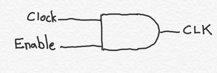
Another relevant sub-topic is clock gaters.
No, not clock gators.
In the prior article in this series where I discussed power consumption, I explained why the switching of signals cause power consumption. An important way to prevent unnecessary power consumption is to prevent memory elements from switching their outputs when their outputs aren’t needed. Clock gating is a design feature where you simply add a logic gate nearby the memory elements. The logic gate accepts the clock as one input, and a “clock enable” (or ”clock disable”) signal as another element. When the memory element is storing a value that is only useful for circuitry that is not needed in a particular clock cycle, you set the enable/disable signal appropriately.
You can either use a separate logic gate or build the enable functionality into the memory itself. The former has the advantage of taking less area and potentially less power consumption if you are controlling multiple memory elements with the same clock gater. If you are not doing so, however, it can be advantageous to build the gating circuitry into the memory element, itself.
Finally, I mentioned that the state elements (memory circuits) can be responsive to the level of the clock or to the edge of the clock. Everyone loves circuit diagrams, so here we go…
First, let’s talk about transmission gates. Transmission gates are tiny little circuits that pass current from one end to the other, or prevent current from passing, depending on an input. This is similar to the way a single transistor works, and sometimes you could just use a single transistor instead, but for the circuits we are talking about it is better to use transmission gates.
On the left, we see a transmission gate. A transmission gate is two transistors wired so that their sources are connected and their drains are connected. One is a PFET and one is an NFET. As we discussed in an earlier article in this series, an NFET is “on” when its gate is at a high voltage, and off when its gate is at a low voltage. A PFET, on the other hand, is on when its gate is at a low voltage and is off when its gate is at a high voltage.
If, as shown here, we connect the two gates to opposite polarities of the same signal - here Clock and !Clock - then both transistors will be on or both will be off. In other words, if Clock is at a high voltage, then, by definition, Clock! is at a low voltage (and vice versa).
As shown in the middle figure above, if we set Clock to a high value (logic 1), then the NFET will be on, and so will the PFET. This allows current to flow from one end of the transmission gate to the other.
And, as shown in the right figure above, if we set Clock to a low value (logic 0), then both the NFET and the PFET will be off, and no current can flow across the transmission gate.
The reason we sometimes use transmission gates instead of just using a single NFET or PFET (we call a single device wired that way a “pass transistor”) is that a transmission gate ensures that the voltage on each side of the gate is the same. If we were to use just an NFET, and assuming the left side is at a high voltage, when the NFET is turned on, the voltage on the left side will be a tiny bit higher than the voltage on the other side. In other words, a single NFET transistor (i.e. half a transmission gate) has difficulty passing a 1 accross itself; it passes what we refer to, sometimes, as a “weak 1.” PFETs, on the other hand, pass weak 0’s. Using both a PFET and an NFET ensures that the voltage is always what it should be, making the circui more immune to noise from external sources.
Now that all that is out of the way, let’s talk about latches. Latches are memory elements that are sensitive to the level of the clock. As long as the clock is a 1, for example, the input is passed to the output of the latch. And as long as the clock is a 0, the input is ignored and the output maintains its pre-existing value.
Below is a very simple latch design, and a design I’ve actually used many times.
You should recognize the presence of not one, but two transmission gates, as well as two inverters. Let’s look at what happens when the clock signal (CLK) is high.
When CLK is high, the left-most transmission gate is turned on, and current can flow through it. So I’ve replaced it with just a wire in the above figure. The other transmission is turned off, so it’s as if there is an open circuit there. For that reason, I’ve simply removed it from the above figure. The net result is a very simple circuit. The input signal, In, passes through an inverter, where it produces In! (the opposite of In) at the output of the circuit. The bottom inverter serves no purpose when the CLK is high, so we can ignore it (it produces an output that doesn’t go anywhere).
So, essentially, as long as CLK is high, the output matches the input (more accurately, it matches the opposite of the input, but to a logic designer this is merely a technicality. We can always add another inverter and flip the signal back to its original form if using its opposite form is inconvenient.)
Now, what happens when the CLK signal is low?
The right transmission gate is on, so I’ve replaced it with a wire. As a result, we have two inverters that are wired in a loop - the output of one is the input to the other. The input to the top inverter will be whatever In was prior to the CLK signal going low. In other words, it’s the prior version of In. The output of that inverter is the opposite of that value. That will also be the input to the bottom inverter. The bottom inverter’s output will invert that again, producing the original value of the prior version of In. We’ve seen, in earlier articles in this series, that this sort of feedback loop can be used to reinforce signals and create memories.
Latches can be used as the main state element (outside of caches, register files and such) in CPUs, and I’ve worked on latch-based designs. They have some beneficial properties; they are small and fast. They also present some challenges. For example, the entire time that the clock signal is high, the input will be captured. If you are using a single-phase clock with a 50% duty cycle, then the latch will be listening for new data through half the clock cycle. It is only the final value that the input has just before the clock signal is set low that ends up getting stored, but the output of the latch will continuously change up until that point and will affect downstream circuits, which may have much less time to calculate their results. This is because only the final value (probably) matters.
To avoid scary design problems it is often preferable to use an edge-triggered memory element; these are often called flip-flops. My favorite kind of flip-flop is what we used to call a “master-slave latch“; to be sensitive to those who may object to this term, other terms are now sometimes used, but it appears that no other term has yet caught on.
The above diagram shows how you can create an edge-triggered master-space latch by connecting two latches. Traditionally, the left latch is called the “master” and the right latch is called the “slave.”
Note that the master and slave are disconnected when CLK is high; regardless of what is going on with the Input, the slave latch is unaffected. It simply stores whatever value it received when the transmission gate on the input of the slave latch was on - that is, when the CLK signal was last low.
Meanwhile, the right, slave latch, is in the opposite configuration because it’s clock signals are wired in reverse. In addition to being disconnected from the master latch, it uses feedback to remember whatever value it received back when the CLK had its opposite value.
If the clock now goes low, the master latch stops paying any attention to what is on its input. It just uses feedback to remember what used to be on its input. And whatever that value is - the value that the master latch remembers - passes through the slave latch to its output. When the clock goes low, the master-slave latch outputs whatever value the master has stored.
When the clock goes high again, the master latch can capture new data. In the meanwhile, the slave latch keeps outputting whatever it was already outputting.
What this all means is that the change in the clock from high to low locks in whatever is on the master-slave latch’s input. This shields the memory element from being affected by changes on the input - the input is captured at a specific instant in time corresponding to a particular transition on the clock.
This is probably a lot more than you wanted to know about clocks and latches and flip-flops, but I had fun writing it!