M3 core counts and performance

dada_dave

Elite Member
Posts
2,300
Reaction score
2,324
View attachment 27209

video confirms @leman 's test and of course the patent he dug up. Very cool, very, very cool.

EDIT: OHHHHHH ... that's how they did it and why the patent kept mentioning cache and DRAM and barely mentioned registers and why they call it Dynamic caching. I admit I only skimmed the patent, but they are now treating a cores registers as another cache. Huh ... that's ... wow ... that's a huge change.


View attachment 27214

Whoa .. continuing on ... they've turned them all into cache! How the hell do they keep the register performance so good treating it as a cache?! What the hell. Man I hope someone deep dives into this GPU.
Hey @theorist9 you know that chips and cheese article you posted on the old Apple GPU, about how it had low L1 cache relative to Nvidia/AMD? I'm going out on a limb here and say the cache structure has probably changed this generation! 🤪


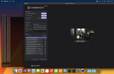
FWIW, Chips and Cheese just posted this analysis of the M2 GPU:
Screen Shot 2023-11-09 at 12.51.31 PM.png

Screen Shot 2023-11-09 at 12.51.41 PM.png


Done! I didn’t suggest he do a write up as that might be a little pushy, but just said he might be interested in it.
Thanks! He had said he was confused (as we all were with the exception of maybe @leman ) by the Dynamic Cache announcement. This clears up so much. And yet poses a whole set of new questions …
 
Last edited:

dada_dave

Elite Member
Posts
2,300
Reaction score
2,324
That second video when they get to occupancy confirms that they turned registers into L1 cache (screenshots in the edited post above) ... I repeat ... how the hell did they do that without trashing performance? Don't get me wrong, L1 cache is fast and *can* be almost as fast as a register, but almost only in an absolute sense - both are very fast, but relative of one to the other, my understanding and maybe I am wrong is that a register is often still 3x faster to access than a cache hit. On the other hand, looking this up, I've seen a couple people claim on CPUs that the latency *can* be equivalent but those claims seem to be in the minority so I don't know under which circumstances it is true, if it is true.

I've also seen people advocate (include Nvidia) for a register cache (for both CPU and GPU systems), but the impression I get from those systems is that there is still a separate register file - i.e. the register cache is in addition to the register file. Maybe for the M3 Apple still has registers in hardware but logically they are part of the L1 cache? - i.e. they still have a register file for the registers but the value isn't there it goes to the L1 cache and there's no logical separation between them?

Nah that doesn't fit. They seem to indicate that the new system has the flexibility to assign as much to thread group memory and function memory as needed and they only ever talk about L1 register file as though it is part of the L1, so it could be but that doesn't seem right.

So maybe they somehow sped up the L1 cache so that it is even faster? Or they take a small hit in access time but the occupancy gains are big enough that it makes up for it? I'm sure Gokhan couldn't comment (Apple secrecy and all that) even if you pinged him on Twitter, but man would I want to anyway if I hadn't nuked my account there. This is really interesting.
 

Aaronage

Power User
Posts
144
Reaction score
213
Getting ahead of myself a bit (impatient and excited!)

Ran a quick Cinebench single thread test to check clocks and CPU/SoC power measured by powermetrics
ST clock: 4.055GHz
CPU Power: ~4.5W

This is way lower than the core power number we saw reported for A17 at just 3.7-3.8GHz.

Interesting! 🤩

Immediate questions are:
1. Is my dumb ass misreading this? 😅
2. Is A17 Pro better than we thought? Did we put too much faith in the geekerwan review and the numbers reported by "spec-on-iOS"?
3. Any chance powermetrics is wrong? I have no reason to believe it's wrong, just curious if anyone doubts this number
I ran Cinebench 2024 single thread with powermetrics polling

CPU power (134 samples):
Average: 4.947W
Max:: 5.58W
Min: 4.34W

Pretty cool! I was concerned Apple would lean on power this generation but that doesn't appear to be the case (again, assuming there's no catch with these numbers).

Of course, with power consumption this low, the machine was stone cold and the fan never spun up. Just the normal Apple Silicon experience really!

The SoC uses around 27W under full CPU load. I believe the 8P+4E M2 Pro used around 34W, so that's a nice win!
 

Attachments

  • Screenshot 2023-11-09 at 22.05.15.png
    Screenshot 2023-11-09 at 22.05.15.png
    362.4 KB · Views: 21

exoticspice1

Site Champ
Posts
310
Reaction score
115
This is absolute bullshit 🙄

I ran Cinebench 2024 single thread with powermetrics polling

CPU power (134 samples):
Average: 4.947W
Max:: 5.58W
Min: 4.34W

Pretty cool! I was concerned Apple would lean on power this generation but that doesn't appear to be the case (again, assuming there's no catch with these numbers).

Of course, with power consumption this low, the machine was stone cold and the fan never spun up. Just the normal Apple Silicon experience really!

The SoC uses around 27W under full CPU load. I believe the 8P+4E M2 Pro used around 34W, so that's a nice win!
can you max out the fans manually and see the ST score you get in Cinebench?
Cause I saw Geekerwan get 148 in ST.
 

Jimmyjames

Site Champ
Posts
772
Reaction score
872
I ran Cinebench 2024 single thread with powermetrics polling

CPU power (134 samples):
Average: 4.947W
Max:: 5.58W
Min: 4.34W

Pretty cool! I was concerned Apple would lean on power this generation but that doesn't appear to be the case (again, assuming there's no catch with these numbers).

Of course, with power consumption this low, the machine was stone cold and the fan never spun up. Just the normal Apple Silicon experience really!

The SoC uses around 27W under full CPU load. I believe the 8P+4E M2 Pro used around 34W, so that's a nice win!
I’m still stunned that a 5 Watt cpu core is beating an i9-14900K one which runs at what…35-50 or even more watts. Crazy.
 

Yoused

up
Posts
5,704
Reaction score
9,105
Location
knee deep in the road apples of the 4 horsemen
L1 cache is fast and *can* be almost as fast as a register, but almost only in an absolute sense - both are very fast, but relative of one to the other, my understanding and maybe I am wrong is that a register is often still 3x faster to access than a cache hit.
The CPU cores store registers in a rename pool, which has some properties that are similar to a cache. It seems possible that the GPU cores may have adopted a simlar design, folding the entire L1 structure into the core itself and tagging cache entries as registers. It could make a lot of sense: put a register tag on a cache entry as a load op, retag it as a dirty cache line as a store op. Cache lines tend to be rather wide things, and GPU operations often work on rather wide data objects (SIMD). The cache line would not be evicted immediately, but chewing through acres of data would get it outta there in due course.
 

Cmaier

Site Master
Staff Member
Site Donor
Top Poster Of Month
Posts
5,492
Reaction score
8,916
That second video when they get to occupancy confirms that they turned registers into L1 cache (screenshots in the edited post above) ... I repeat ... how the hell did they do that without trashing performance? Don't get me wrong, L1 cache is fast and *can* be almost as fast as a register, but almost only in an absolute sense - both are very fast, but relative of one to the other, my understanding and maybe I am wrong is that a register is often still 3x faster to access than a cache hit. On the other hand, looking this up, I've seen a couple people claim on CPUs that the latency *can* be equivalent but those claims seem to be in the minority so I don't know under which circumstances it is true, if it is true.

Typically registers are at least 10x faster than cache. But I think what they’re getting at here is that they are caching registers, not that the local register file has gone away. They just use cache algorithms to try and ensure that the register file holds the values it is most likely to need soon.
 

dada_dave

Elite Member
Posts
2,300
Reaction score
2,324
The CPU cores store registers in a rename pool, which has some properties that are similar to a cache. It seems possible that the GPU cores may have adopted a simlar design, folding the entire L1 structure into the core itself and tagging cache entries as registers. It could make a lot of sense: put a register tag on a cache entry as a load op, retag it as a dirty cache line as a store op. Cache lines tend to be rather wide things, and GPU operations often work on rather wide data objects (SIMD). The cache line would not be evicted immediately, but chewing through acres of data would get it outta there in due course.
Very interesting! Thanks! Bringing the cache inside the core … would any of this be visible in released die shots or is L1 structure too small? I’m very much not familiar with what you can see and what you can’t. I know L2 and so forth tend to be big enough to see but would such a physical reorganization be clear on a die shot or not really? It put annother way even if you could see it you wouldn’t be able to meaningfully distinguish how an M2 GPU is using its L1 cache vs how the M3 is?

Typically registers are at least 10x faster than cache. But I think what they’re getting at here is that they are caching registers, not that the local register file has gone away. They just use cache algorithms to try and ensure that the register file holds the values it is most likely to need soon.

Very cool. So your hypothesis is the same as my first one, the registers/register file still exists, but logically they’ve been folded into the L1 cache. I discounted it because of the wording in the presentations but on top level presentations maybe I shouldn’t read too much into that and for performance I have to agree that it makes the most sense barring some magical new tech to make the L1 super fast.

But is that still mutually exclusive with @Yoused ‘s idea that they brought the L1 inside the core? If they are logically part of the same pool would you design them to be physically collocated? Or is that not necessary if they’re simply part of the same logical structure but they don’t have to share physical space?
 

dada_dave

Elite Member
Posts
2,300
Reaction score
2,324
I'm sure Gokhan couldn't comment (Apple secrecy and all that) even if you pinged him on Twitter, but man would I want to anyway if I hadn't nuked my account there. This is really interesting.
turns out he’s on mastodon. I’ve pinged him and will post if I get a reply!
 

Jimmyjames

Site Champ
Posts
772
Reaction score
872
turns out he’s on mastodon. I’ve pinged him and will post if I get a reply!
It’ll be interesting to see if he replies. My experience is Apple employees basically never reply to unsolicited questions. Perhaps the one exception is NatBro (Nat Brown). He came over from Valve and now heads the Game Technologies effort I think. Controllers, GPTK etc. He’s usually really open and responsive.

Edit: Or maybe he’ll be more open now...
1699576580315.png


Edit2: @dada_dave you’ve started me down this rabbit hole! This is a very interesting statement.
1699576691644.png
 
Last edited:

dada_dave

Elite Member
Posts
2,300
Reaction score
2,324
It’ll be interesting to see if he replies. My experience is Apple employees basically never reply to unsolicited questions. Perhaps the one exception is NatBro (Nat Brown). He came over from Valve and now heads the Game Technologies effort I think. Controllers, GPTK etc. He’s usually really open and responsive.
I’m not expecting anything either. But you never know …
 

Cmaier

Site Master
Staff Member
Site Donor
Top Poster Of Month
Posts
5,492
Reaction score
8,916
Very cool. So your hypothesis is the same as my first one, the registers/register file still exists, but logically they’ve been folded into the L1 cache.

Well, it’s more that the only logical structure is registers, and they are physically implemented as a local register file that is cached. The caching is transparent to the programmer, who logically sees only registers. I assume.
 

dada_dave

Elite Member
Posts
2,300
Reaction score
2,324
It’ll be interesting to see if he replies. My experience is Apple employees basically never reply to unsolicited questions. Perhaps the one exception is NatBro (Nat Brown). He came over from Valve and now heads the Game Technologies effort I think. Controllers, GPTK etc. He’s usually really open and responsive.

Edit: Or maybe he’ll be more open now...
View attachment 27221

Edit2: @dada_dave you’ve started me down this rabbit hole! This is a very interesting statement.
View attachment 27222
Do you have a link? I can’t seem to see those posts.

Well, it’s more that the only logical structure is registers, and they are physically implemented as a local register file that is cached. The caching is transparent to the programmer, who logically sees only registers. I assume.

Hmmm I’m not quite sure I understand, I’ll think about it though. Like I get the part that the programmer doesn’t have to explicitly worry about the implementation and would see what they expect as just registers as registers, but I’m confused by the statement that the only logical structure is registers. The whole L1 cache is surely not just a giant registry file? Or am I completely confused by what you’re saying?
 

dada_dave

Elite Member
Posts
2,300
Reaction score
2,324
Sure. I edited my post with the links.
When I login to the mastodon app I don’t see any of those responses. Makes me wonder what else I’m missing! I also wonder if I have some setting that’s causing this? I only see his top level posts.
 

Cmaier

Site Master
Staff Member
Site Donor
Top Poster Of Month
Posts
5,492
Reaction score
8,916
Do you have a link? I can’t seem to see those posts.


Hmmm I’m not quite sure I understand, I’ll think about it though. Like I get the part that the programmer doesn’t have to explicitly worry about the implementation and would see what they expect as just registers as registers, but I’m confused by the statement that the only logical structure is registers. The whole L1 cache is surely not just a giant registry file? Or am I completely confused by what you’re saying?
“Logical” refers to “what does the programmer see?” Logically there are registers. Physically they are implemented as a complex hybrid system of small and big SRAMs and logic that shifts things back and forth.

(A register file is essentially a small SRAM. A cache is a big one.)
 

dada_dave

Elite Member
Posts
2,300
Reaction score
2,324
“Logical” refers to “what does the programmer see?” Logically there are registers. Physically they are implemented as a complex hybrid system of small and big SRAMs and logic that shifts things back and forth.

(A register file is essentially a small SRAM. A cache is a big one.)
I think I got it now. This is what I was envisioning. They talk about how the overall “L1 cache” can be flexibly partitioned to use exactly what the programmer needs - the programmer will be in logic dealing with register data, thread group storage, cache buffer, stack, etc … and the new system has these all in the same effective pool of memory partitioning up the small and large SRAMs that make up that pool as necessary. But that raises all sorts of questions then too.

If your register file cache extends beyond the bounds of the small SRAM normally reserved for the registers and into the larger SRAM of what is traditionally the L1 one presumes there is a performance drop off accessing that extra data - just as it would accessing a formally higher level cache. Knowing where that boundary is could still be a useful point of reference for optimization. So how big is that small vs large SRAM?

Further does this mean the L1 partition for the register cache has a minimum size, the small SRAM, or can the other core memory data types mentioned extend into that smaller, faster cache?

I’m sure I can think of more but those are the two main ones and why I initially discounted the idea of multiple SRAMs making up this one pool. The top level talks made it sound like there’s just one big SRAM where everything can be dumped. But I can’t think of how that would be performant. There’s a reason we have a small faster SRAM for registers and a larger one for L1 cache.
 

Altaic

Power User
Posts
146
Reaction score
183
If your register file cache extends beyond the bounds of the small SRAM normally reserved for the registers and into the larger SRAM of what is traditionally the L1 one presumes there is a performance drop off accessing that extra data - just as it would accessing a formally higher level cache. Knowing where that boundary is could still be a useful point of reference for optimization. So how big is that small vs large SRAM?
That's what I was thinking... At some point, high occupancy saturates the ALU and extra small SRAM doesn't help. One would want enough small SRAM that the ALU can be busy while additional computations' registers are swapped from the large SRAM, thus hiding large SRAM latency. I could be totally off-base, though 😅
 
Top Bottom
1 2