In Part 4 I explained that when it comes to memory, you essentially have to trade off capacity vs. speed. If you want a large pool of available memory, it will tend to be slow compared to a small pool of memory. I also explained that you can take advantage of this trade-off by using multiple memories; for example a small, very fast, register file can be used to store data that is of immediate use, and then, when the data is not going to be needed again any time soon, it can be put back into the large, but slow, main memory.
I also explained that, with a register file, the software has to be aware of this mechanism, and has to decide when to store something in registers and when to store something in main memory.
Caches are memory systems that work on the same principle - using smaller, faster memories whenever you can - but are (more or less) transparent to software. The CPU contains logic that tries to automatically put data in the cache when it is likely to be needed, and removes it when it is not likely to be needed in the near future.
In any modern computer, there is a memory hierarchy that starts with the processor and its register file, includes at least one level, if not more, of cache, main memory, and what I referred to in 1996 as “external storage” (referring then to things like disk drives, but now more likely to be something like flash memory, SSDs, or even networked storage).
When the CPU needs to write a memory location, it also checks the cache. If the cache currently is storing a copy of that memory location, the data can be stored in the cache, where, if it is needed again, the CPU can read it later. At some point the data also has to be written to main memory. Until that happens, the contents of that memory address in the cache are said to be dirty. A dirty cache entry is a cache entry that has been modified by the CPU, but has not yet been written to the main memory. For caches that serve all CPU cores (which may mean it just serves the one and only CPU core), the main reason to ”clean” the cache and write data into main memory is when you run out of space in the cache and have to replace some of its contents with different memory addresses; if you replace a dirty cache entry with the contents of a different memory address without writing the data to main memory, you will lose those changes. That’s a bad thing.
If you have multiple CPU cores, each with its own cache, then you have a different problem, called coherency. If core0 writes a value into address XXX into its cache, and core1 reads the value at address XXX from its own cache, those two values may end up not being the same. When core0 writes the value into XXX, there has to be some way for all the other cores to know that any value they have in their cache for address XXX is wrong. This is a topic for another day.
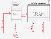
 The above diagram illustrates, at a very high level, the architectural behavior of a cache. The CPU has a set of buses and signals that it can use to communicate with the memory subsystem. This must always include an address bus, which is a set of wires that specifies which location in the memory is to be read from or written to. It’s important to remember that this address is not an address local to the cache; it’s a main memory address. In other words, address 0x1000 in the main memory may be found at any address in the cache; the CPU only needs to know the address in the main memory, and it is up to the cache to keep track of whether or not it has a copy of main memory’s address 0x1000, and, if so, where it put it.
There must also always be a data bus, which is used to send data to the memory or receive data from the memory. Finally, there must be some sort of signal, above called “read/write,” which is used to tell the memory whether to send data to the CPU (“read”) or to accept data from the CPU (“write”).
The cache, itself, needs to have a similar (in functionality at least) set of buses and signals for communication with the memory (or, in the alternative, to a second level of cache).
When the cache receives a request to read out an address to the CPU, it will do so, so long as it possesses the contents of that address in its own memory. If not, then there are several possibilities. The way this particular diagram is drawn, the cache would presumably ask the main memory for the appropriate data, then, once it receives it, it would store it in itself and send a copy to the CPU. In reality, this may, instead, be implemented in a manner such that the cache tells the CPU that it didn’t have the data (i.e. that there was a cache miss) so that the CPU knows it has to wait for main memory to return the data. Instead of the cache asking main memory for the data, the CPU may do so instead. These are all implementation decisions that depend on many factors. However, the following modified block diagram shows one practical way this may work.

Here we’ve made two modifications. First, the cache informs the CPU, via a “Hit/Miss” wire, whether the requested memory address is stored in the cache or not. This is useful for the CPU since it needs to know how long the memory access will take. The second modification, shown by the red arrow on the left, is that the CPU, when it sends a read request to the cache, simultaneously sends it to the main memory (or whatever memory the cache talks to). This way that memory can get a head start fetching the data, and doesn’t have to wait for the cache to figure out whether or not it already has it. This can save a bunch of CPU cycles, depending on the design implementation, and there is generally no harm in the memory beginning a read that is not needed; if power consumption is a concern, however, some power can be save by preventing the main memory reads until we are sure we really need them.
Let’s assume, for a moment, that the cache keeps track of memory address in a 1:1 fashion. In other words, the memory is a series of rows, each row corresponding to one single address (e.g. 64 bits wide). As we’ll see, this is almost never the case, but it will simplify the discussion for the moment. In that case, the cache might look something like this:

There are two primary components to a cache. The first is the SRAM that stores copies of the contents of main memory for whatever subset of addresses are being handled by the cache. If we are assuming a very simple cache for a 64-bit CPU, and we decide that each address in the cache’s SRAM corresponds to a single address in the main memory (which we’ll see is not a great idea), then this SRAM may be 65 bits wide; the first 64 bits correspond to the memory data (for example, copies of the data from main memory). The extra, 65th bit, is for keeping track of whether the cache entry is dirty. (Note: the dirty status could be kept in a different memory structure, depending on implementation).
The other main cache component is a content-addressable memory, or CAM. This is a special kind of memory structure that words like a hash structure in software, for those who are familiar with data structures. A CAM is a structure that tells you whether or not it is storing a particular piece of data. You don’t have to know where the CAM might be storing the data - you merely ask it whether it has the data anywhere. This is all possibly best understood by analogy that explains the difference between a RAM and a CAM. Using a RAM is like knowing that someone interesting lives at a particular street address. You know the street address but you don’t know who’s in the house. Using the street address, you go to the house, ring the bell, and see who answers.
A CAM, on the other hand, is essentially the reverse. You think that Spider-Man lives somewhere in your town, but you aren’t sure, and you don’t know where. So you drive around town with a megaphone and yell “Spider-Man!” everywhere you go, until either you’ve covered the whole town without a response (in which case you get a cache miss), or until Spider-Man turns on his porch light in response to your maniacal screaming, thereby informing you of where he lives.
The cache’s CAM receives data (in this case, the desired main memory address), and tells you whether or not that address is stored in the CAM. If so, data associated with the input data is output. So, in this case, the CAM receives the desired main memory address, and outputs a localized cache address; in other words, it outputs the location in the cache’s SRAM that holds the data associated with that main memory address. If the address is not found in the CAM, then the CAM produces a signal which can be forwarded to the CPU to indicate a cache miss; it can also be used to trigger a read of the main memory.
Let’s consider an example.

In the figure above, our CPU has sent the address 0x1000 to the cache, because it wants to read the data from that location in main memory. The CAM actually does contain the number 0x1000, in row 2. As a result, it changes the voltage an output wire corresponding to row 2 (shown in red) which is connected to the SRAM. In this case, since each row of the CAM has its own output wire, these can correspond to the wordlines of the SRAM, which tells the SRAM which address to read (the one corresponding to row 2). The resulting data, 1001001, is read from the SRAM, and sent to the CPU on the data bus.
There are a couple of things to note here. In this case I’ve designed the cache so that if address 0x1000 is stored in row 2 of the CAM, then the data corresponding to address 0x1000 must be stored in row 2 of the SRAM. This does not have to be the case; I could make a more complicated system where the CAM contains additional memory cells that keep track of an address in the SRAM, and then send an address to the SRAM instead of a single wire for each row. In my example, the close coupling between the CAM and SRAM - the fact that their rows correspond - means that I am likely to design the CAM and SRAM into a single structure, saving a bit more space. In a sense, the CAM is just a different addressing mechanism for accessing the SRAM. Instead of receiving an address and using logic circuits to decide which wordline to turn on in the SRAM, we just receive a different kind of address, and use that to figure out which wordline to turn on.
Another thing to note is that the addresses in the CAM are in a random order. Typically, when your cache starts out empty, you start at the top and put the first address you are asked to deal with in row 0, then the next one in row 1, etc. Once all your rows are filled, if you are asked to access a new memory address, you must replace one of the existing addresses. There are many methods for dealing with this, which will be discussed later.
Returning to our example above, the CPU asked to read address 0x1000. Spatial locality tells us that the CPU is very likely to soon want to access neighboring memory addresses, like, say, 0x1001 or 0x1002.
To take advantage of this, let’s redesign our cache a little bit.

Here, what I’ve done, is that I’ve modified the SRAM so that instead of storing the contents of a single memory address in each row, it stores the concept of four different memory addresses in each row. To make this easier to understand, I’ve also switched to using binary memory addresses instead of hexadecimal.
In this case, the memory addresses are 7 bits long (not realistic, but this is just a toy example). If I were to list out all possible 7-bit memory addresses, the list would start out like this:
If I want to group these into groups of four, I can find the first entry in each group of four by ignoring the bottom (e.g. the rightmost) two bits. For example:
If I look at the five-most left bits of each address, the first four all are at block address 00000. The next four all are at block address 00001.
If I wanted to have groups of two, instead I could just ignore the single rightmost bit. For groups of eight, I could just ignore the three rightmost bits. In other words, I can group into groups containing any power-of-two number of entries by ignoring some number of right-most bits.
In the example above, the CPU wants to read the contents of main memory at address 1001000. To read the CAM, only the top five bits are read: 10010. This is found in row 2. That means that row 2 of the SRAM will hold the contents of memory addresses 1001000, 1001001, 1001010, and 1001011.
Assuming that the CPU only wants one of those addresses (which may or may not be the case; for example, for instruction caches, it may be helpful to send a number of sequential instructions at once to the CPU), the lower two bits (in this case 00) are used by circuitry (which I’ve indicated as the Column Picker) to decide which of the four entries in the row is to be sent to the CPU. In this case, that is the left-most of the four columns in the SRAM.
If the cache did not contain the requested address, it would request it from the main memory and then store it. Unlike our earlier examples, however, it will store four consecutive addresses at once, and not just the single address being requested. Assuming that the bus between the main memory and the cache is big enough to send data for four addresses at once, this can save a lot of time. Instead of:
Fetch X from main memory
Fetch X+1 from main memory
Fetch X+2 from main memory
Fetch X+3 from main memory
The system need merely do:
Fetch X, X+1, X+2 and X+3 from main memory
This takes ¼ the time, assuming that the CPU actually needs the data stored at each of those addresses at some point.
Note that the bus width between the cache and the main memory does not have to be the same width as the data stored in the cache. This is a technical trade off that depends on many factors, including RAM architecture, physical limitations in running large numbers of parallel wires, etc.
Essentially, if any address can be mapped to any row, then the cache is said to be associative. If, instead, there is a simple mapping between main memory address and cache memory address (for example, by ignoring the leftmost address bits), the cache is said to be direct-mapped.
Direct-mapped caches are simpler and faster to access, but tend to result in many more cache misses, so overall worse system performance. In practice, real caches that I’ve seen have been associative. The examples above have also been associative, as any address can be mapped to any row.
There are many strategies for deciding which existing entry to replace; these are called replacement algorithms. Let’s first consider the ideal replacement algorithm. Ideally, if you had perfect knowledge, and you had to remove an existing entry from the cache, you would remove the entry that is not going to be needed for the longest time. If there is one entry that I‘m going to need the next clock cycle, and another entry that I’m never going to use again, you should get rid of the one that you are never going to use. If there is one entry that I’m going to need the next clock cycle, and another that won’t be needed for 100 cycles, then you should get rid of the one that isn’t going to be needed for 100 cycles.
Unfortunately, perfect knowledge, like the frictionless ball bearing and massless pulley, doesn’t exist.
Instead, we typically use something called Least Recently Used (LRU). The LRU algorithm is designed to take advantage of temporal locality and usually performs quite well. The idea behind LRU is that when you remove an entry from the cache, you remove the entry that hasn’t been used for the longest time. The idea behind this is that you tend to use a particular memory address multiple times within a given time period. The longer that it has been since the last time you used that memory address, the more likely it is that you are done with that memory address and aren’t going to use it again.
There are variations of LRU where you estimate which entry is the least recently used, instead of keeping detailed tracking information, or you can keep careful track of which entry is the least recently used. Deciding exactly what algorithm to use requires trading off hardware issues (power, speed, area) vs. cache performance. A little inaccuracy may have no effect on cache hit rate but may reduce power substantially.
If we are going to design a true LRU algorithm in hardware, there are many ways to do it. One method is to include something like a counter, that increments each time a cache access occurs. When a cache row is accessed, the value of that counter is stored with that cache row. When it comes time to replace a row, you replace the row with the lowest counter number associated with it. [Note: this is more complicated than it appears, because the counter would be designed to wrap around to start at 0 again, and it takes time to find the lowest counter number unless you also simultaneously keep track of that].
An alternative technique would be to use a shift register that keeps a list of cache rows sorted by when they were last used, and adjusts the list after every access; this can also be complicated because unlike a normal shift register, which simply shifts every item to the left, any given entry may have to move all the way to the right with only the entries after it shifted to the left.
In any case, LRU is an algorithm that is absolutely possible to implement, and while the hardware to do so is not incredibly simple, the trade off is generally worth it, and, in my experience LRU or LRU-adjacent algorithms are commonly used in caches.
There are many other potential algorithms. These include, for example:
For this reason, it is very common to have multiple levels of cache, each (usually) being bigger than the preceding one as you move further and further away from the CPU. (Another oft-violated rule of thumb is that each level of cache is 2x the size of the prior one).
Since the level 2 cache is bigger than the level 3 cache, it will still hold many of the entries that have been removed from the level 1 cache by replacement. The following is an incredibly oversimplified example, where we have an L1 Cache with 2 rows, and an L2 Cache with 4 rows:
 Let’s assume the caches are both empty, and the CPU attempts to read memory address 1000. What will happen is that the L1 Cache will miss and the CPU will have to try the L2 Cache. The L2 Cache will also miss, so the CPU will have to read address 1000 from main memory. As part of that process, the contents of address 1000 will be stored in both the L2 and L1 Caches.

Next, the CPU asks for memory address 3000. Since neither cache contains the contents of address 3000, it will have to be fetched from main memory, and will then be stored in both caches.

Next, the CPU attempts to read the contents of memory address 7FFF. Once again, neither cache contains the contents of memory address 7FFF, so main memory is read. The data corresponding to address 7FFF is stored in the L2 Cache. But now the L1 Cache is out of space, and it must replace the contents of one of its rows with the contents of memory address 7FFF. Assuming we are using the Least Recently Used algorithm, the L1 Cache will get rid of (or as Intel seems to like to put it, “victimize”) the data corresponding memory address 1000.

Now, if the CPU wants to read address 1000, unfortunately it can not do so from the L1 Cache. It can, however, read it from the L2 Cache. This isn’t ideal, but it’s much better than having to fetch it from main memory.
There has been some academic research, and some industrial toying around, with so-called “victim caches,” which are specifically designed to hold items that have been evicted from various levels of cache. In situations where the caches are specifically tied to a single CPU core, this seems to me to be of limited value, as the next level of cache will hold those ”victimized” entries, anyway. If there are multiple cores sharing a cache (say a level 2 cache), then it could make more sense to have a dedicated victim cache. An example follows, picking up from our prior example:

Here we have two L1 Caches, corresponding to two CPU cores. These two L1 Caches both share an L2 Cache. Imagine CPU1, the bottom one, asks for memory address 7F55. This is not in the L2 Cache or the L1 Cache, so it will be fetched from main memory (and eventually end up in CPU1’s L1 Cache). The L2 Cache has no room to store it unless it throws something away. In this case, if it is using the Least Recently Used algorithm it may throw away the row containing the contents of address 1000. In that case, when CPU0 wants to read memory address 1000, it cannot rely on it being in the L2 Cache - it will have to read it from main memory.
A ”victim cache,” which is a cache that just holds items that have been replaced, can mitigate against this sort of problem when you have multiple cores interacting like this. And, of course, there are other circumstances where multiple L1 caches share an L2 cache - for example, where, as is typically the case, a particular core has separate instruction and data level 1 caches, but a single, shared, L2 cache.
Whether or not a victim cache is worth the trouble depends on how often it is that you discard things from a cache only to need it again soon. You may be better off increasing the size of a cache so that you don’t have to discard as often. Victim caches tend to be level 3 or level 4 caches, so it takes quite awhile to read them, though still less than the time it takes to read main memory. Whether or not to use a victim cache is a decision that cannot easily be made without considering many different alternative memory architectures and simulating them with real and intended instruction streams to try and figure out what makes the most sense. It is my understanding, though, that while level 3 caches are not to uncommon, victim caches are not widely used.
The first instruction puts the contents of register 1 in memory address FF00. The second instruction puts the contents of register 2 in memory address FF00, overwriting what we just wrote there.
Later on we read the contents of address FF00 into register 3.
If every time we perform a store to memory we put the data not just into the cache but also into main memory, we will waste power, and maybe time. When we wrote R1 into address FF00, that data was never needed - it was replaced by different data in the next instruction - so writing it into memory would have been a waste of time. (We are assuming a single CPU core, and that there isn't some other core somewhere that wants to consume that value stored in address FF00.
As a result, one solution is to never write the contents of the cache into main memory until that address is about to be removed from the cache. If our cache replacement algorithm is about to remove address FF00 from the cache and the contents of the cache corresponding to address FF00 have never been written to m main memory, then that data would be lost forever. Therefore it is not uncommon to do these sorts of "lazy" writes to the main memory when the cache is about to evict a dirty address.
Another scheme is to scan the cache, looking for dirty entries, and writing them one at a time into main memory when nothing else is trying to access main memory; the goal in this case is to keep the main memory reasonably up-to-date without causing a bandwidth backlog.
Schemes in which memory is immediately updated every time a write occurs are called write-through schemes. Schemes in which memory is update later are called write-back schemes. Write-back schemes generally perform better and consume less power, but require more complicated hardware.
As was mentioned earlier, a related problem is cache synchronization. When you have multiple CPU cores (or CPU and GPU cores) that are accessing a unified memory address space, when CPU0 reads a memory address it should see any changes made to that address by CPU1, even if those changes have not been reflected yet in main memory. There are many schemes for accomplishing this, but generally they involve communication between caches so that even if a cache isn't aware of the correct contents of an address, it at least knows that it's own copy is wrong.
A second difference is the memory access pattern. Data memory is accessed in an arbitrary manner - the same memory address may be accessed many times in a row, then another memory address very distant from the first may be accessed. The pattern is usually not truly random, or even pseudorandom, but it’s certainly often hard to predict.
Instruction memory, on the other hand, is typically read in a sequential fashion. The CPU contains a counter called a “program counter,” that contains the memory address of the instruction which is to be executed. Most of the time, when an instruction is executed, the program counter increments so as to point at the next sequential memory address.
One exception would be when when a branch occurs. The instruction stream may contain instructions that cause jumps to instructions at memory locations that are not in sequence. These may be unconditional branch instructions (i.e. “Jump to memory location XXXX”) or conditional branch instructions (i.e. “if the contents of register 1 is 0x0000, jump to memory location YYYY”).
It turns out that conditional branches are almost always taken. In other words, if you were to see a conditional branch instruction in the instruction stream and had to guess as to whether the condition would be satisfied such that the instruction stream will make a jump, you’d do very very well by guessing “yes.”
Finally, the addresses used for the instruction stream tend to very different than the ones used for data - it’s considered a very bad idea to intermingle instructions and data in memory, for security and other reasons.
For these reasons, typically you would have separate instruction and data caches, as indicated in the diagram below:

Because instruction memory accesses are different than data memory accesses, the instruction cache will likely be designed differently from the data cache. First, there is no need to worry about what happens when you write into memory from the CPU. Second, because you will tend toward sequential memory accesses, the instruction cache may be "wider" than the data cache, with the ability to store and handle larger blocks of memory addresses simultaneously.


For commercial designs, we have the advantage of being able to instrument actual designs with real software and operating systems to capture cache hit rates (and miss rates). This enables the designer to identify places where performance suffers due to the design of the cache memories. Nonetheless, software simulation is quite common, since the solution to performance problems is not always intuitive; increasing a cache size may increase cache read times and have a less beneficial effect than shrinking a cache to allow the next level of cache to be placed closer to the CPU, for example. Designers try many potential designs before settling on a design that hopefully maximizes performance of whatever the designer is using as benchmarks for the design.
I also explained that, with a register file, the software has to be aware of this mechanism, and has to decide when to store something in registers and when to store something in main memory.
Caches are memory systems that work on the same principle - using smaller, faster memories whenever you can - but are (more or less) transparent to software. The CPU contains logic that tries to automatically put data in the cache when it is likely to be needed, and removes it when it is not likely to be needed in the near future.
In any modern computer, there is a memory hierarchy that starts with the processor and its register file, includes at least one level, if not more, of cache, main memory, and what I referred to in 1996 as “external storage” (referring then to things like disk drives, but now more likely to be something like flash memory, SSDs, or even networked storage).

Locality
The fundamental principle that allows caches to be useful is called locality. In particular, there are two types of locality which, when present, allow a cache to be useful; by “useful,” I mean that, as long as these types of locality are in effect, a cache will likely greatly speed up the operation of your CPU.- Temporal locality - this refers to the fact that when the CPU needs a piece of data or a variable from memory, it will tend to need that data again soon. For example, when a memory location is read from memory, often the data will be manipulated and new data will be written into the same memory location. This is because each memory location represents a variable in the software source code. (For data caches at least - instruction caches operate a little differently but similar principles apply).
- Spatial locality — if a memory location is needed by the CPU, other memory locations nearby will tend to be needed soon. All of the variables used by a software program, for example, tend to be stored close together. Data structures like arrays tend to be stored in sequential memory locations. When source code uses object-oriented principles, different attributes of the same object tend to be stored in consecutive memory addresses.
Basic Operation
Fundamentally, the idea is that the cache is transparent to software. When the CPU needs to read a memory location, it checks the cache. If the cache has a copy of that memory location, it can read the contents of the cache instead of, and much more quickly than, “main memory.” This is called a cache hit. A cache hit occurs when the address the CPU is looking for is available in the cache, and therefore no access to main memory is required.When the CPU needs to write a memory location, it also checks the cache. If the cache currently is storing a copy of that memory location, the data can be stored in the cache, where, if it is needed again, the CPU can read it later. At some point the data also has to be written to main memory. Until that happens, the contents of that memory address in the cache are said to be dirty. A dirty cache entry is a cache entry that has been modified by the CPU, but has not yet been written to the main memory. For caches that serve all CPU cores (which may mean it just serves the one and only CPU core), the main reason to ”clean” the cache and write data into main memory is when you run out of space in the cache and have to replace some of its contents with different memory addresses; if you replace a dirty cache entry with the contents of a different memory address without writing the data to main memory, you will lose those changes. That’s a bad thing.
If you have multiple CPU cores, each with its own cache, then you have a different problem, called coherency. If core0 writes a value into address XXX into its cache, and core1 reads the value at address XXX from its own cache, those two values may end up not being the same. When core0 writes the value into XXX, there has to be some way for all the other cores to know that any value they have in their cache for address XXX is wrong. This is a topic for another day.
There must also always be a data bus, which is used to send data to the memory or receive data from the memory. Finally, there must be some sort of signal, above called “read/write,” which is used to tell the memory whether to send data to the CPU (“read”) or to accept data from the CPU (“write”).
The cache, itself, needs to have a similar (in functionality at least) set of buses and signals for communication with the memory (or, in the alternative, to a second level of cache).
When the cache receives a request to read out an address to the CPU, it will do so, so long as it possesses the contents of that address in its own memory. If not, then there are several possibilities. The way this particular diagram is drawn, the cache would presumably ask the main memory for the appropriate data, then, once it receives it, it would store it in itself and send a copy to the CPU. In reality, this may, instead, be implemented in a manner such that the cache tells the CPU that it didn’t have the data (i.e. that there was a cache miss) so that the CPU knows it has to wait for main memory to return the data. Instead of the cache asking main memory for the data, the CPU may do so instead. These are all implementation decisions that depend on many factors. However, the following modified block diagram shows one practical way this may work.
Here we’ve made two modifications. First, the cache informs the CPU, via a “Hit/Miss” wire, whether the requested memory address is stored in the cache or not. This is useful for the CPU since it needs to know how long the memory access will take. The second modification, shown by the red arrow on the left, is that the CPU, when it sends a read request to the cache, simultaneously sends it to the main memory (or whatever memory the cache talks to). This way that memory can get a head start fetching the data, and doesn’t have to wait for the cache to figure out whether or not it already has it. This can save a bunch of CPU cycles, depending on the design implementation, and there is generally no harm in the memory beginning a read that is not needed; if power consumption is a concern, however, some power can be save by preventing the main memory reads until we are sure we really need them.
Cache Components
To accomplish these functions, the cache needs a way to keep track of what memory addresses it contains, and where it put them. It also needs to keep track of whether or not each address is dirty. As I discussed earlier, an address is dirty if it has been modified and not yet saved to main memory. It’s important to keep track of dirty addresses so that the cache doesn’t remove them from its memory without first writing the result into memory, otherwise the memory value will be wrong if it is ever read again.Let’s assume, for a moment, that the cache keeps track of memory address in a 1:1 fashion. In other words, the memory is a series of rows, each row corresponding to one single address (e.g. 64 bits wide). As we’ll see, this is almost never the case, but it will simplify the discussion for the moment. In that case, the cache might look something like this:
There are two primary components to a cache. The first is the SRAM that stores copies of the contents of main memory for whatever subset of addresses are being handled by the cache. If we are assuming a very simple cache for a 64-bit CPU, and we decide that each address in the cache’s SRAM corresponds to a single address in the main memory (which we’ll see is not a great idea), then this SRAM may be 65 bits wide; the first 64 bits correspond to the memory data (for example, copies of the data from main memory). The extra, 65th bit, is for keeping track of whether the cache entry is dirty. (Note: the dirty status could be kept in a different memory structure, depending on implementation).
The other main cache component is a content-addressable memory, or CAM. This is a special kind of memory structure that words like a hash structure in software, for those who are familiar with data structures. A CAM is a structure that tells you whether or not it is storing a particular piece of data. You don’t have to know where the CAM might be storing the data - you merely ask it whether it has the data anywhere. This is all possibly best understood by analogy that explains the difference between a RAM and a CAM. Using a RAM is like knowing that someone interesting lives at a particular street address. You know the street address but you don’t know who’s in the house. Using the street address, you go to the house, ring the bell, and see who answers.
A CAM, on the other hand, is essentially the reverse. You think that Spider-Man lives somewhere in your town, but you aren’t sure, and you don’t know where. So you drive around town with a megaphone and yell “Spider-Man!” everywhere you go, until either you’ve covered the whole town without a response (in which case you get a cache miss), or until Spider-Man turns on his porch light in response to your maniacal screaming, thereby informing you of where he lives.
The cache’s CAM receives data (in this case, the desired main memory address), and tells you whether or not that address is stored in the CAM. If so, data associated with the input data is output. So, in this case, the CAM receives the desired main memory address, and outputs a localized cache address; in other words, it outputs the location in the cache’s SRAM that holds the data associated with that main memory address. If the address is not found in the CAM, then the CAM produces a signal which can be forwarded to the CPU to indicate a cache miss; it can also be used to trigger a read of the main memory.
Let’s consider an example.
In the figure above, our CPU has sent the address 0x1000 to the cache, because it wants to read the data from that location in main memory. The CAM actually does contain the number 0x1000, in row 2. As a result, it changes the voltage an output wire corresponding to row 2 (shown in red) which is connected to the SRAM. In this case, since each row of the CAM has its own output wire, these can correspond to the wordlines of the SRAM, which tells the SRAM which address to read (the one corresponding to row 2). The resulting data, 1001001, is read from the SRAM, and sent to the CPU on the data bus.
There are a couple of things to note here. In this case I’ve designed the cache so that if address 0x1000 is stored in row 2 of the CAM, then the data corresponding to address 0x1000 must be stored in row 2 of the SRAM. This does not have to be the case; I could make a more complicated system where the CAM contains additional memory cells that keep track of an address in the SRAM, and then send an address to the SRAM instead of a single wire for each row. In my example, the close coupling between the CAM and SRAM - the fact that their rows correspond - means that I am likely to design the CAM and SRAM into a single structure, saving a bit more space. In a sense, the CAM is just a different addressing mechanism for accessing the SRAM. Instead of receiving an address and using logic circuits to decide which wordline to turn on in the SRAM, we just receive a different kind of address, and use that to figure out which wordline to turn on.
Another thing to note is that the addresses in the CAM are in a random order. Typically, when your cache starts out empty, you start at the top and put the first address you are asked to deal with in row 0, then the next one in row 1, etc. Once all your rows are filled, if you are asked to access a new memory address, you must replace one of the existing addresses. There are many methods for dealing with this, which will be discussed later.
Block Size
The examples above are great for taking advantage of temporal locality. If I access a memory location, that memory location will be available (at least for awhile) in the cache, so that the next time I need it I don’t need to read all the way from main memory. But the other kind of locality, spatial locality, is also important, and by modifying our design we can greatly improve our results.Returning to our example above, the CPU asked to read address 0x1000. Spatial locality tells us that the CPU is very likely to soon want to access neighboring memory addresses, like, say, 0x1001 or 0x1002.
To take advantage of this, let’s redesign our cache a little bit.
Here, what I’ve done, is that I’ve modified the SRAM so that instead of storing the contents of a single memory address in each row, it stores the concept of four different memory addresses in each row. To make this easier to understand, I’ve also switched to using binary memory addresses instead of hexadecimal.
In this case, the memory addresses are 7 bits long (not realistic, but this is just a toy example). If I were to list out all possible 7-bit memory addresses, the list would start out like this:
0000000
0000001
0000010
0000011
0000100
0000101
0000110
0000111
If I want to group these into groups of four, I can find the first entry in each group of four by ignoring the bottom (e.g. the rightmost) two bits. For example:
00000[00]
00000[01]
00000[10]
00000[11]
———————————————
00001[00]
00001[01]
00001[10]
00001[11]
If I look at the five-most left bits of each address, the first four all are at block address 00000. The next four all are at block address 00001.
If I wanted to have groups of two, instead I could just ignore the single rightmost bit. For groups of eight, I could just ignore the three rightmost bits. In other words, I can group into groups containing any power-of-two number of entries by ignoring some number of right-most bits.
In the example above, the CPU wants to read the contents of main memory at address 1001000. To read the CAM, only the top five bits are read: 10010. This is found in row 2. That means that row 2 of the SRAM will hold the contents of memory addresses 1001000, 1001001, 1001010, and 1001011.
Assuming that the CPU only wants one of those addresses (which may or may not be the case; for example, for instruction caches, it may be helpful to send a number of sequential instructions at once to the CPU), the lower two bits (in this case 00) are used by circuitry (which I’ve indicated as the Column Picker) to decide which of the four entries in the row is to be sent to the CPU. In this case, that is the left-most of the four columns in the SRAM.
If the cache did not contain the requested address, it would request it from the main memory and then store it. Unlike our earlier examples, however, it will store four consecutive addresses at once, and not just the single address being requested. Assuming that the bus between the main memory and the cache is big enough to send data for four addresses at once, this can save a lot of time. Instead of:
Fetch X from main memory
Fetch X+1 from main memory
Fetch X+2 from main memory
Fetch X+3 from main memory
The system need merely do:
Fetch X, X+1, X+2 and X+3 from main memory
This takes ¼ the time, assuming that the CPU actually needs the data stored at each of those addresses at some point.
Note that the bus width between the cache and the main memory does not have to be the same width as the data stored in the cache. This is a technical trade off that depends on many factors, including RAM architecture, physical limitations in running large numbers of parallel wires, etc.
Associativity
I haven’t talked much about how the cache decides where (i.e., in which row), to store the data associated with a particular memory address. In cache design we talk about two kinds of caches: direct-mapped caches and set-associative caches.Essentially, if any address can be mapped to any row, then the cache is said to be associative. If, instead, there is a simple mapping between main memory address and cache memory address (for example, by ignoring the leftmost address bits), the cache is said to be direct-mapped.
Direct-mapped caches are simpler and faster to access, but tend to result in many more cache misses, so overall worse system performance. In practice, real caches that I’ve seen have been associative. The examples above have also been associative, as any address can be mapped to any row.
Replacement Algorithms
As discussed above, the cache must sometimes decide how to replace one cache entry with another. If the cache is full, but the CPU wants access to a new address that is not already in the cache, then the new data has to replace some existing data in the cache. The cache will always be smaller than main memory, so it’s impossible to store the contents of every address in main memory in the cache. A particular software program may or may not fit within the cache; if it doesn’t, then, while it is running, entries will have to be swapped in and out of the cache.There are many strategies for deciding which existing entry to replace; these are called replacement algorithms. Let’s first consider the ideal replacement algorithm. Ideally, if you had perfect knowledge, and you had to remove an existing entry from the cache, you would remove the entry that is not going to be needed for the longest time. If there is one entry that I‘m going to need the next clock cycle, and another entry that I’m never going to use again, you should get rid of the one that you are never going to use. If there is one entry that I’m going to need the next clock cycle, and another that won’t be needed for 100 cycles, then you should get rid of the one that isn’t going to be needed for 100 cycles.
Unfortunately, perfect knowledge, like the frictionless ball bearing and massless pulley, doesn’t exist.
Instead, we typically use something called Least Recently Used (LRU). The LRU algorithm is designed to take advantage of temporal locality and usually performs quite well. The idea behind LRU is that when you remove an entry from the cache, you remove the entry that hasn’t been used for the longest time. The idea behind this is that you tend to use a particular memory address multiple times within a given time period. The longer that it has been since the last time you used that memory address, the more likely it is that you are done with that memory address and aren’t going to use it again.
There are variations of LRU where you estimate which entry is the least recently used, instead of keeping detailed tracking information, or you can keep careful track of which entry is the least recently used. Deciding exactly what algorithm to use requires trading off hardware issues (power, speed, area) vs. cache performance. A little inaccuracy may have no effect on cache hit rate but may reduce power substantially.
If we are going to design a true LRU algorithm in hardware, there are many ways to do it. One method is to include something like a counter, that increments each time a cache access occurs. When a cache row is accessed, the value of that counter is stored with that cache row. When it comes time to replace a row, you replace the row with the lowest counter number associated with it. [Note: this is more complicated than it appears, because the counter would be designed to wrap around to start at 0 again, and it takes time to find the lowest counter number unless you also simultaneously keep track of that].
An alternative technique would be to use a shift register that keeps a list of cache rows sorted by when they were last used, and adjusts the list after every access; this can also be complicated because unlike a normal shift register, which simply shifts every item to the left, any given entry may have to move all the way to the right with only the entries after it shifted to the left.
In any case, LRU is an algorithm that is absolutely possible to implement, and while the hardware to do so is not incredibly simple, the trade off is generally worth it, and, in my experience LRU or LRU-adjacent algorithms are commonly used in caches.
There are many other potential algorithms. These include, for example:
- FIFO: first in first out. Get rid of the oldest item you stored in the cache, regardless of how recently it was used. This is simpler to design, but will likely have worse performance than LRU.
- MRU: most recently used. For certain types of software, this can have better performance than LRU. This is mostly an academic algorithm, and I’m not aware of it ever being used in real hardware.
- LFU: least frequently used. Get rid of the entry that is used most infrequently. The idea is that if I’ve used a memory address many times, chances are I’m going to keep needing to use it. The hardware for this is not too dissimilar from LRU.
Replacement Victims
After a row in the cache is replaced, what happens to the the data that used to be there? Rest assured, the data is never lost. The data is still available somewhere, but where depends on the overall system architecture. If there is only a single level of cache, then, in order to retrieve the data that fell victim to a replacement algorithm, you have to fetch it from main memory. The cost of this is power and time. Instead of reading just the cache, you have to transmit a request to the main memory and read that, too, which burns power. And reading the main memory takes much longer than reading the cache (an oft-violated rule-of-thumb is that each time you have to go one level further out to fetch the data, it takes 10x as long as reading the prior level).For this reason, it is very common to have multiple levels of cache, each (usually) being bigger than the preceding one as you move further and further away from the CPU. (Another oft-violated rule of thumb is that each level of cache is 2x the size of the prior one).
Since the level 2 cache is bigger than the level 3 cache, it will still hold many of the entries that have been removed from the level 1 cache by replacement. The following is an incredibly oversimplified example, where we have an L1 Cache with 2 rows, and an L2 Cache with 4 rows:
Next, the CPU asks for memory address 3000. Since neither cache contains the contents of address 3000, it will have to be fetched from main memory, and will then be stored in both caches.
Next, the CPU attempts to read the contents of memory address 7FFF. Once again, neither cache contains the contents of memory address 7FFF, so main memory is read. The data corresponding to address 7FFF is stored in the L2 Cache. But now the L1 Cache is out of space, and it must replace the contents of one of its rows with the contents of memory address 7FFF. Assuming we are using the Least Recently Used algorithm, the L1 Cache will get rid of (or as Intel seems to like to put it, “victimize”) the data corresponding memory address 1000.
Now, if the CPU wants to read address 1000, unfortunately it can not do so from the L1 Cache. It can, however, read it from the L2 Cache. This isn’t ideal, but it’s much better than having to fetch it from main memory.
There has been some academic research, and some industrial toying around, with so-called “victim caches,” which are specifically designed to hold items that have been evicted from various levels of cache. In situations where the caches are specifically tied to a single CPU core, this seems to me to be of limited value, as the next level of cache will hold those ”victimized” entries, anyway. If there are multiple cores sharing a cache (say a level 2 cache), then it could make more sense to have a dedicated victim cache. An example follows, picking up from our prior example:
Here we have two L1 Caches, corresponding to two CPU cores. These two L1 Caches both share an L2 Cache. Imagine CPU1, the bottom one, asks for memory address 7F55. This is not in the L2 Cache or the L1 Cache, so it will be fetched from main memory (and eventually end up in CPU1’s L1 Cache). The L2 Cache has no room to store it unless it throws something away. In this case, if it is using the Least Recently Used algorithm it may throw away the row containing the contents of address 1000. In that case, when CPU0 wants to read memory address 1000, it cannot rely on it being in the L2 Cache - it will have to read it from main memory.
A ”victim cache,” which is a cache that just holds items that have been replaced, can mitigate against this sort of problem when you have multiple cores interacting like this. And, of course, there are other circumstances where multiple L1 caches share an L2 cache - for example, where, as is typically the case, a particular core has separate instruction and data level 1 caches, but a single, shared, L2 cache.
Whether or not a victim cache is worth the trouble depends on how often it is that you discard things from a cache only to need it again soon. You may be better off increasing the size of a cache so that you don’t have to discard as often. Victim caches tend to be level 3 or level 4 caches, so it takes quite awhile to read them, though still less than the time it takes to read main memory. Whether or not to use a victim cache is a decision that cannot easily be made without considering many different alternative memory architectures and simulating them with real and intended instruction streams to try and figure out what makes the most sense. It is my understanding, though, that while level 3 caches are not to uncommon, victim caches are not widely used.
Write Policies
When the CPU writes something to memory, the cache will capture that data and associate it with the relevant address. The question is whether or not you also write that information into main memory at the same time. Consider the following sequence of instructions:store R1 -> [FF00]
store R2 -> [FF00]
...
load [FF00] -> R3The first instruction puts the contents of register 1 in memory address FF00. The second instruction puts the contents of register 2 in memory address FF00, overwriting what we just wrote there.
Later on we read the contents of address FF00 into register 3.
If every time we perform a store to memory we put the data not just into the cache but also into main memory, we will waste power, and maybe time. When we wrote R1 into address FF00, that data was never needed - it was replaced by different data in the next instruction - so writing it into memory would have been a waste of time. (We are assuming a single CPU core, and that there isn't some other core somewhere that wants to consume that value stored in address FF00.
As a result, one solution is to never write the contents of the cache into main memory until that address is about to be removed from the cache. If our cache replacement algorithm is about to remove address FF00 from the cache and the contents of the cache corresponding to address FF00 have never been written to m main memory, then that data would be lost forever. Therefore it is not uncommon to do these sorts of "lazy" writes to the main memory when the cache is about to evict a dirty address.
Another scheme is to scan the cache, looking for dirty entries, and writing them one at a time into main memory when nothing else is trying to access main memory; the goal in this case is to keep the main memory reasonably up-to-date without causing a bandwidth backlog.
Schemes in which memory is immediately updated every time a write occurs are called write-through schemes. Schemes in which memory is update later are called write-back schemes. Write-back schemes generally perform better and consume less power, but require more complicated hardware.
As was mentioned earlier, a related problem is cache synchronization. When you have multiple CPU cores (or CPU and GPU cores) that are accessing a unified memory address space, when CPU0 reads a memory address it should see any changes made to that address by CPU1, even if those changes have not been reflected yet in main memory. There are many schemes for accomplishing this, but generally they involve communication between caches so that even if a cache isn't aware of the correct contents of an address, it at least knows that it's own copy is wrong.
Instruction Caches
The way that a CPU accesses memory to retrieve instructions is very different than the way that a CPU accesses memory to deal with data. First, most CPUs don’t modify the instruction stream. In other words, instructions flow in one direction - from the memory to the CPU. Data, on the other hand, is both read from memory and written to it by the CPU.A second difference is the memory access pattern. Data memory is accessed in an arbitrary manner - the same memory address may be accessed many times in a row, then another memory address very distant from the first may be accessed. The pattern is usually not truly random, or even pseudorandom, but it’s certainly often hard to predict.
Instruction memory, on the other hand, is typically read in a sequential fashion. The CPU contains a counter called a “program counter,” that contains the memory address of the instruction which is to be executed. Most of the time, when an instruction is executed, the program counter increments so as to point at the next sequential memory address.
One exception would be when when a branch occurs. The instruction stream may contain instructions that cause jumps to instructions at memory locations that are not in sequence. These may be unconditional branch instructions (i.e. “Jump to memory location XXXX”) or conditional branch instructions (i.e. “if the contents of register 1 is 0x0000, jump to memory location YYYY”).
It turns out that conditional branches are almost always taken. In other words, if you were to see a conditional branch instruction in the instruction stream and had to guess as to whether the condition would be satisfied such that the instruction stream will make a jump, you’d do very very well by guessing “yes.”
Finally, the addresses used for the instruction stream tend to very different than the ones used for data - it’s considered a very bad idea to intermingle instructions and data in memory, for security and other reasons.
For these reasons, typically you would have separate instruction and data caches, as indicated in the diagram below:
Designing for Performance
It is difficult to determine the performance characteristics of a cache design without simulating it; performance will be heavily dependent on the workload (the specific software being run, and the data that the software is using). As a cache designer, I created software that provided a rough simulation of the CPU’s memory access characteristics and pipelines, and which accepted as inputs information about the memory hierarchy (cache and memory access times, cache sizes, memory bus width, cache organization (associativity, block sizes, etc.) and “cache traces” that represented memory access patterns by specific software applications that were frequently used as benchmarks (such as gcc, SPICE, etc.) The output of the simulation provided information about cache hit rate, average memory access times, and other memory performance characteristics. Running thousands of simulations provided feedback to allow me to choose cache characteristics based on graphs such as these:For commercial designs, we have the advantage of being able to instrument actual designs with real software and operating systems to capture cache hit rates (and miss rates). This enables the designer to identify places where performance suffers due to the design of the cache memories. Nonetheless, software simulation is quite common, since the solution to performance problems is not always intuitive; increasing a cache size may increase cache read times and have a less beneficial effect than shrinking a cache to allow the next level of cache to be placed closer to the CPU, for example. Designers try many potential designs before settling on a design that hopefully maximizes performance of whatever the designer is using as benchmarks for the design.