If you have a logical function that needs to be implemented, how do you break that down into the logic gates that correspond to “standard cells” in order to actually implement the design with transistors? There are certainly automated ways to do this. For example, nearly everyone (apart from very high end CPU designers) uses Synopsys’ logic compiler tools to do this. But every CPU designer, and certainly CPU designers working on the most cutting-edge designs, needs to understand how to work with logic functions, how to ”minimize” and refactor them, and how to replace gates with other gates in order to reduce area and power consumption, or to increase performance.
The easiest way to understand these techniques is to work through an actual problem. When I was but a wee undergrad engineering student, professor Jack Fitzgerald McDonald, in his hardware design class, gave us an assignment. Each of us was to design and build a functional electronic die. This consisted of some LEDs, representing each of the pips corresponding to a die face. There was also a button. Press and hold the button and the die face started flashing through different possible values very quickly. Release the button and the die stops and displays between 1 and 6 pips. To do this I used a 555-timer chip, a bunch of logic gate chips, a couple of NAND gates to de-bounce the push button, and a lot of little wires.
We’ll use that as inspiration for a slightly different problem, addressing a 7-segment LED.

These things are (or used to be) ubiquitous. Every clock radio, digital clock, lots of signs, etc. use variations of this thing. Above we have a 7-segment LED, with an 8th element (a decimal point). The segments are labeled from A to G.
Depending on what number you are displaying, different segments are turned on. Let’s look at segment A. It is lit up for some, but not all, digits:

From the image above, we see that segment A is lit up for the following digits: 0, 2, 3, 5, 6, 7, 8 and 9. It is not lit up for digits 1 and 4.
Now, imagine that we have a binary counter that can output, in sequence, integer values, starting at 0. The decimal value and the corresponding binary equivalent are shown below, in the form of a truth table:

The way this table is read is that inputs to the logic function are on the left (here the decimal value is in the leftmost column and the binary equivalent is in the middle column) and outputs are in the right column.
We only care about the digits 0 through 9, because that’s all you can display in a single 7-segment LED. The counter will have four output wires: b3, b2, b1, b0. We will assume that the digit we want to display on the 7-segment LED will correspond to the decimal value corresponding to those four wires arranged in that order. (This mapping is arbitrary. If I wanted to, I could have the LED display 4 when the counter outputs 6, or whatever. In some cases, rearranging things in such a way can be useful; it may reduce circuit noise or power consumption, or the number of gates required. This is something else that logic designers must consider, but I don’t want to bite off more than we can chew in this article).
Note that we have four output wires from the counter, which means we can have 16 possible output values, but we are only using 10 of them. We don’t care about the remaining values. Don’t care is a wonderful term-of-art in logic design. It means that for certain combinations of input values, we really don’t care what the output is. This means that we don’t have to work hard to try to make those outputs have any particulate value when those input combinations are active, freeing us from having to include yet more logic to address those combinations. Often times we use the symbol “d” or it’s greek equivalent to represent don’t care in truth tables and when working with logic equations.
I can’t emphasize enough how excited I get by don’t cares. Many times I have run into thorny problems meeting my timing goals and found that I could solve the problem by realizing that there were don’t cares that the architect didn’t notice (or chose to ignore). What happens is that the architect who writes the high level behavioral model for the chip can easily write smaller logic equations by ignoring don’t cares. If some combination of inputs is impossible, for example, it is easier to just ignore that possibility when writing the architectural model than it is to specifically call that out by making the logic more complicated and treating the don’t cares separately. Often times I would stare at the logic for a long time and realize there were hidden don’t cares that I could take advantage of.

Above, I have augmented the table to add don’t cares. We are going to use the heck out of those.
The first technique taught to fledgling logic monkeys is the Karnaugh Map. The Karnaugh Map is a useful logic minimization technique as long as you have three or four inputs. It’s possible to use with five or six inputs, and I’ve done it a few times, but it’s not a lot of fun; it’s literally a bit like 3D chess in that case.
We have four inputs - b3, b2, b1, and b0 - so we are good to go with a Karnaugh Map.

Above is the Karnaugh Map for our problem. Along the left side are b3 and b2 and along the top are b1 and b0. So, for example, if we are looking for the case where b3 b2 b1 b0 = 1101, then that is the third row down (where b3 b2 = 11) and the second column from the left (where b1 b0 = 01).
Inside each square, we put a 0, a 1, or a d, depending on the value from our truth table (the right-most column from the tables at the top of this article).
Note that the rows and columns proceed in a funny order. Normally, when counting in binary, we would count like this: 00, 01, 10, 11. Here we are counting 00, 01, 11, 10. This type of counting, called Gray coding, has fun properties that help the Karnaugh Map work. The idea is that each neighbor differs by only 1 digit. That also includes when we wrap around - 00 differs from 01 by one digit, but it also differs from 10 by one digit.
There are two ways to use a Karnaugh Map - it can be used to produce what is called a “Sum of Products” or to produce a “Product of Sums” (SOP or POS, respectively). For some reason, young logic designers seem to always prefer SOP, so we’ll start there.
To find the SOP form from a Karnaugh Map, we try to find the biggest rectangle we can that contains only 1’s. The quantity of squares in the rectangle must be a power-of-2. In other words, the rectangle we identify must have 16, 8, 4, 2, or 1 squares in it. Since we want to find a big rectangle, we treat the d’s as if they are 1’s - that improves the likelihood that we can make a bigger rectangle. Note that you can wrap around when finding the rectangle. That is, you can start in the fourth column and then include squares from the first column. We will have an example of that in a bit.
We have a couple of choices for the biggest rectangle containing only 1’s and d’s, so below I have picked one:

Here I’ve drawn a red rectangle containing 8 squares. 8 is a power of 2, so that works. I can’t make the rectangle any bigger without including a 0, and that would be illegal. I could have, instead, drawn a rectangle around the bottom two rows. In the end, this choice doesn’t matter, because both options include 8 squares.
Next I repeat the process, until all of the 1’s in the Karnaugh Map exist inside a rectangle. I don’t have to include all the d’s, but whenever convenient I can treat d’s as 1’s.
Below I’ve drawn the next biggest rectangle I can draw that includes 1’s that were not already captured by a rectangle. I did this with the blue rectangle:

Note that my rectangles overlap. That’s perfectly fine. At this point I have two more 1’s, at the top left, that are not yet in rectangles. So I keep going.

This time I‘ve draw a green square. That sucked in one of those rogue 1’s. The square covers four entries In the map, and 4 is a power of 2. That’s why I couldn’t extend the square to the right or down to include more 1’s (or d’s). That would result in a rectangle covering 6 squares, and 6 is not a power of 2. And I can’t extend the bottom right corner of the green square to the bottom right corner of the map, because then I would have 9 entries in my square, and 9 is not a power of 2.
I now have one more 1 left to capture:

This time I made a rectangle in yellow, covering two different entries in the map. I did this by wrapping the rectangle around from the left column to the right column. I did promise we’d see a wrapping example, after all. The number 2, of course, is a power of 2, so this works.
Now I am done. I have no more 1’s left to capture. Usually, at that point, I’d head across the street from AMD and get a burrito. But I assume you already have a burrito, so we’ll move on to our next steps.
What we need to do is look at one rectangle at a time, and for that rectangle, figure out what values of b3, b2, b1, and b0 do not change. Pay close attention here and you’ll get it, no problem.
Let’s start with the yellow rectangle. The yellow rectangle covers these two values of b3 b2 b1 b0: 0000 and 0010. You can tell simply by reading the values of the left and top sides of the Karnaugh Map. The top left square is at b3 b2 = 00 and b1b0 = 00 (concatenating those gives 0000). The top right square is at b3 b2 = 00 and b1 b0 = 10 (giving us 0010).
So we have two values: 0000 and 0010. Which digits are identical between those two values? These: 00-0. The first, second and last. The third digit does change - it’s a 0 in the left square and a 1 in the right square. The digits that match each other correspond to b3, b2, and b0. As a result, we can extract a “product” (remember: we are doing “sum of products”) corresponding to b3, b2 and b0 and ignoring b1. Since the digits are 0’s, and we are doing SOP form, we need to invert b3 b2 and b0. If the digits were 1’s, we wouldn’t invert. If the digits were 0’s but we were doing POS, we wouldn’t invert (but we would also be covering 0’s, not 1’s, with our rectangles).
That means that the product, or min term (Boolean math has some crazy nomenclature), corresponding to the yellow rectangle is b3’ b2’ b0’. These are written without any operator between them, like you’d write multiplication of variables in algebra - hence the name “product.” The apostrophe after each variable is a way of saying “the inversion of this variable.” We would read this as “b3 prime” or “not b3,” depending on preference. Logic designers have way too many ways of indicating inversion - apostrophes, lines over the variable, prefacing or suffixing with exclamation points, prefacing with a tilde… Sorry about that.
The implied operator is the Boolean AND function. What we are saying is that if we AND together b3’, b2’ and b0’ and get a 1, then the LED segment should be lit up. In other words, if b3’, b2’ AND b0’ are all 1’s, then the segment is lit. Which is another way of saying that b3, b2 and b0 all being 0’s means the segment is lit; because b3 is the opposite of b3’, b2 is the opposite of b2’ and b0 is the opposite of b0’.
Note that if any of the products evaluates to true (i.e. a 1), then the segment lights up. And each product corresponds to one of our rectangles.
To save you from scrolling, here’s our Karnaugh Map again. Let’s look at the green square. It corresponds to four values of b3 b2 b1 b0: 0101, 0111, 1101, and 1111. We need to identify which digits of those four values are identical across all four values. The left-most digit, corresponding to b3, is sometimes a 0 and sometimes a 1. So we ignore that. The next digit, corresponding to b2, is always a 1. So we keep that. The next digit, corresponding to b1, is sometimes a 0 and sometimes a 1, so we ignore that. And the right-most digit, corresponding to b0, is always a 1, so now we know that our answer will involve b2 and b0, because those two bit positions never change. We also see that each is always a 1. Since we are doing SOP and these are 1’s, we do not have to invert. That means that our second product, which corresponds to the green square, is b2 b0. If b2 and b0 are both 1’s, then our LED segment should turn on.
Note that we have a pattern developing. Our first rectangle had 2 entries in it, and produced a product with 3 variables in it. Our second rectangle had 4 entries in it, but produced a product with only 2 variables in it. So far it looks like maybe the bigger the rectangle, the smaller the product. Smaller products require less logic - fewer transistors and less power consumption - to implement.
The remaining two rectangles each cover 8 entries. Let’s do the blue one.
Here are the values of b3 b2 b1 b0 that are covered by the blue rectangle:
There is only one column where the value doesn’t change: b3. Since the value in that column is always a 1 and we are doing SOP, then our product is simply b3. If b3 is a 1, then our segment should light up.
Finally our red rectangle. I‘ll leave this as an exercise for the reader to prove, but the only input that doesn’t change is b1, which is always 1. So if b1 is a 1, then our segment should light up.
What we do next is we write out our sum of the four products we just found:

We’ve just written a “sum of products,” reduced form of the logic equation that gives us the truth table we started with. The “+” operator means ”Boolean OR.” (As usual, there are many ways to write an “OR,” including a ”v,” a “|,” and probably a bunch of other symbols that aren’t currently coming to mind. (Logic designers borrow from many disciplines, including math, physics, computer science, etc. We end up being fluent enough in all of them that we mix and match terminology in ways that would give a pure mathematician or a pure computer scientist heartburn).
This equation may seem fairly complicated, but let’s compare that to the naive SOP representation that we can automatically derive from the original truth table - to do that, we simply sum up the products that correspond to each row that has a 1 in its output column:

That expression in blue in the right column - ”summing” eight terms, each of which has four variables, is the canonical form of the logic equation corresponding to our desired function. Obviously, the result of our Karnaugh Map analysis is much simpler. But - is it right? Let’s double-check that.

In the above truth table, I’ve added two new sections. Remember, for the minimized logic equation to be correct, it must produce the same values as are shown in the red column. It must produce a 1 whenever the LED segment should be lit, and a 0 otherwise. We don’t care what results we get for the rows that are marked “d,” because these are don’t cares.
In the first new section, I added a column for each of the four products in our sum of products. The first column is simply b1. The second column is b3. The third column is the product b2 b0. The “product” is produced by performing the Boolean AND function; this means it produces a 1 only when both b2 and b0 are 1’s. Otherwise it produces a 0.
The fourth column corresponds to the final term, b3’ b2’ b0’. This produces a 1 only when b3, b2 and b0 are 0 (because we need to invert each value before we perform the Boolean AND).
The right-most section of the above table is the “sum” of the four products. This “sum” is really a Boolean OR operation; it means that the result is a 1 only if any of the four products is a 1. You can see from the blue column that the answer is correct; it matches the red column perfectly (if we ignore the “d” entries).
I intentionally made a mistake above. Did you catch it? I did It to make our analysis more interesting, but as a result of this mistake, the answer is not actually the smallest expression that we could obtain. So let’s fix the mistake and try again.
If you look at the yellow rectangle, you will remember that I wrapped off the left and right sides of the map. But I can also wrap off the top and bottom! That would give us the following Karnaugh Map:

Now our yellow rectangle is a square that covers the four corners of our Karnaugh Map. That means we need to revisit the product corresponding to the yellow rectangle. What stays constant in those four yellow squares? In all four, b2 is 0. And in all four, b0 is 0. So, the term would be b2’ b0’.
That means, our corrected sum of products from this Karnaugh Map is: b1 + b3 + b2 b0 + b2’ b0’. That’s a little simpler, because we were able to make one of our rectangles a little bigger. We are going to prove that this logic expression is correct later on in this article, when we arrive at the same solution using a completely different method.
That said, let’s look at how you do a Karnaugh Map to produce a POS expression.
First, here’s our Karnaugh Map again:
This time we are going to produce rectangles that cover the 0’s, and not the 1’s. We can treat the d’s as 0’s to make it possible to make larger rectangles. This time our rectangles won’t be able to be so big. The biggest rectangle we can make is the red rectangle below, which covers b3 b2 b1 b1 = 0100 and 1100.

We learned earlier that bigger rectangles make for shorter terms (in this case instead of products, we have sums. And the sums are sometimes called maxterms. Because, once again, logic designers like to use all the nomenclature they can find.). The don’t cares help us in this case; otherwise we would have no rectangle bigger than a single entry.
We still have one more 0 to cover. That’s done below with the nice blue square.

Now we will look at one rectangle at a time and extract a sum for each. This time, we invert if the corresponding bits in the inputs are 1’s, instead of 0’s.
Looking at the red rectangle, we said our entries corresponded to 0100 and 1100. The first bit differs between the two, but b2, b1 and b0 are the same. So these bits will be part of our sum. We need to invert b2, because in both entries b2 is a 1. So, our first sum is b2’ + b1 + b0.
For the blue square, we end up with b3 + b2 + b1 + b0’ (I’ll leave that as an exercise for the reader).
Our overall product of sums, therefore, is (b2’ + b1 + b0)(b3 + b2 + b1 + b0’).
The following truth table tests our result.

Each of the two sums has its own column. Remember that a “sum” is the logical OR of its terms. Meaning that the result is 1 if any of the terms (taking into account any indicated inversions) is a 1. The final answer, the “product” (which is the logical AND of the two sums) is shown in the right-most column. If we ignore the don’t cares (as we should), the results perfectly match the desired results (shown in the Segment A column).

If we have 5 or 6 inputs, we need to go in 3-dimensions, like 3D chess:

Here I’ve shown a partial 5-input Karnaugh Map. I have two 4-input Karnaugh Maps, that are tied together. One of the two corresponds to when b4=0 and the other corresponds to when b4=1. I’ve shown a red and blue square/rectangle that span across the two maps. The green rectangle is found on only one of the two maps, corresponding to b4=1. I also indicated the minterms (the products) corresponding to each; I’ll leave their derivation to the reader.
If I have 6 inputs, I would stack four maps, each corresponding to a pair of values for the 5th and 6th board. I could keep going, but then I‘d need to think in four dimensions or more. It quickly gets to the point where using a Karnaugh Map becomes impractical. Which brings us to the next technique.

We start by looking at our truth table again. We will only pay attention to rows where the output is a 1 or a don’t care (hence the red lines through the two rows where the output is a 0).
We are going to look at the inputs corresponding to each row that remains after we cross out the 0-rows, and count how many 1’s there are. For example, the first row, corresponding to digit 0, has no 1’s among b3, b2, b1 or b0. The row corresponding to digit 2 has a single 1 (corresponding to b1). Etc. We are going to group the rows together based on how many 1’s are in the inputs for each row, as follows:

The left column is how many 1’s are in the inputs in that group. The middle column is shorthand for each row from the truth table: d0 means the row for digit 0, and d8 means the row for digit 8, for example. If the row was a don’t care row, I put it in parentheses (just to keep track of it). The right column is the set of inputs (b3 b2 b1 b0) corresponding to that digit/row. So, for example, in our truth table we saw that we had a row for digit 8, which corresponded to the set of inputs 1000. There is a single 1 in that set of inputs. So in the table, in group 1 (corresponding to a single 1 in the inputs), we have d8 and 1000.
This grouping isn’t strictly necessary, but it makes the algorithm a little easier to do when you are doing it by hand; as you’ll see, in subsequent steps it means we only have to work in one direction - downward - which makes things less confusing.
Our next step will be to find what are called implicants. These are sort of like the rectangles we found in the Karnaugh Maps, but not quite. We will repeat the search for implicants in stages. First we will find “size 2” implicants, then “size 4,” then ”size 8,” etc. We stop when we can’t go any further.
So, how do we find size 2 implicants? We walk through the table above, looking at our binary inputs, and finding rows that match except for exactly one difference. Let’s do some examples.
Let’s start with d0, which corresponds to 0000. We start going downward, row-by-row, until we find a binary string that differs in only one position. So, for example, d2, which is 0010, differs from 0000 in only one position. We therefore can combine these two entries into a size-2 implicants, which we can write as d(0,2) and the binary string 00-0 (or 00d0, or 00x0, or whatever nomenclature makes you happy). The dash (“-”) goes in the bit position that has a different value between d0 and d2.
Now we keep going, looking for more rows we can combine with d0. It turns out that d8 is 1000, so we can create an implicants d(0,8) with binary string -000. We put the dash in the first position because d0 has a 0 in that position and d8 has a 1 in that position.
At this point we can stop looking for things to combine with d0. Remember that you must have one and only one difference between the rows we are combining. Since d0 has no 1’s in it, and d2 and d8 have a single 1 in them, we can combine them. But anything from the subsequent groups will have at least two 1’s in the binary strings. Going from all 0’s to a string with two 1’s in it means at least two bit positions must differ, which means we can’t combine.
So far we have this:

We’ve created a new column for the size-2 implicants. We found two such implicants, both involving d0 on the one hand and an entry from the “1” group from our previous table on the other hand.
Returning to our prior table, next we look at d2, which corresponds to binary string 0010. Because we organized our table Into groups based on the number of 1’s in the binary strings, we only have to look down the table, and don’t have to look at group 0 anymore.
We can’t combine d2 (0010) with d8 (1000) because there are two bits that differ between those binary strings; the first bit and the third bit. So we keep looking downward, in group 2.
d3 (0011) differs from d2 (0010) in only one bit position - the rightmost one. We can create an implicant d(2,3) with pattern 001- by combining d2 and d3.
If we keep going, we’ll see that d2 (0010) and d5 (0101) differ in 3 positions, so we can’t combine them. We can, however, combine d2 (0010) with d6 (0110) to create d(2,6) (0-10). We‘ll also find that d(2,10) works, which I’ll leave to the reader to prove.
Once we run out of things to combine with d2, we look at d8. Below, I’ve written the implicants that correspond to group 0 and group 1. Feel free to double-check my work.

We keep doing this, going group-by-group and row-by-row, until we reach the bottom. This gives us the following table:

You can already see why this is a lot more tedious than Karnaugh Maps, at least for four inputs, and we’re not close to done yet.
Next we are going to find size-4 implicants. Finding size-4 implicants is similar to finding size-2 implicants, but instead of looking at our original binary column, we look at the binary patterns in the size-2 implicants column. We treat dashes as “must match.” So, for example, we could combine 110- and 100- because they have a dash in the same (rightmost) bit position, and there is only 1 difference in the remaining bit positions (the second bit from the left). We would therefore combine 110- and 100- into 1-0-, placing a second dash in the bit position where there is a difference between the binary strings.
So, let’s start at the top of our list of size-2 implicants:
d(0,2) has a dash in the third position. We can only combine it with other size-2 implicants that also have a dash in the third position. Look downward through our list, the first possibility is d(5,7):

I’ve put red boxes around each size-2 implicant with a dash in the third position; all of them have at least two 1’s, but d(0,2) has no 1’s. This means that all of them differ from d(0,2) in at least 2 bit positions. So, looking at d(5,7) (01-1) and comparing it to d(0,2) (00-0), we see that the rightmost bit differs, and so does the second bit from the left. Therefore these cannot be combined. The same is true of all the other candidates. Therefore d(0,2) cannot be part of a size-4 implicant, and we move on to d(0,8).

This time I’ve cropped our table to only show up through group 1; the groups below group 1 will have at least two 1’s in every entry, and d(0,8) has zero 1’s. We need a single 1 otherwise more than one bit position will differ from d(0,8).
d(2,10) is our only candidate in group 1. d(0,8) (-000) differs from d(2,10) (-010) only in a single position - the second from the right. As a result we can combine these two size-2 implicants into a size-4 implicants: d(0,8,2,10) which has bit pattern -0-0. The second dash is because d(0,8) has a 0 in that position whereas d(2,10) has a 1.
This also means we have accounted for d0, d2, d8, and d10 from our list of digits (In the second column of our table). By the time we are done, we need to have accounted for every digit that corresponds to a 1 on the output: 0, 2, 3, 5, 6, 7, 8, 9. We don’t care about the aptly-named don’t cares. So, in other words, in the “Digit” column of our grouped table, we care about each Digit that is not in parentheses. I bring this up now because, recall, d(0,2) couldn’t be combined with anything. Once we run out of combinations we can make, we need to decide which implicants make our final list. Our list could have some size-8 implicants, some size-4 implicants, and some size-2 implicants, for example. If d0 or d2 is not found in a big implicant (a size-4 or size-8, say), then we would have to include d(0,2) in our final list of implicants, even though it is a puny size-2 implicant.
In any event, we continue this process, moving on to d(2,3), then d(2,6), etc. We find as many size-4 implicants as we can. Then we go through each size-4 implicant and try to combine them to create size-8 implicants. Then we try to make size-16 implicants. This is the point where I pull the finished pot roast from the oven and skip over an hour’s worth of work:

As you can see, we have some size-8 implicants, but we can go no further; none of the size-8 implicants can be combined. There are a couple more things to note.
First, you will notice that some implicants have a red line through them. These are duplicates - they are the same as other implicants, just with the list of digits in a different order. If I was doing this exercise for real and not for explaining to others, each time I created an implicant I would sort the list of digits. So d(0,8,2,10) would be d(0,2,8,10). The order doesn’t matter. Sorting helps identify duplicates and makes it easier to keep track of which digits I have managed to cover. The downside is it makes it harder to keep track of what I combined in order to make the bigger implicants.
In any event, we can ignore the duplicates; regardless of the order of the digits in the implicants, the bit patterns will be the same.
Second, you will see that some of the size-4 implicants are written in red. Earlier I mentioned that we may need to include smaller implicants in our final list, if they cover digits that the bigger implicants don’t cover. That’s what the red implicants are. For example, d(0,8,2,10) is in red. If you look at the size-8 implicants, you can see that none of them cover digit 0. In order to include digit 0 in our final answer, therefore, we need to include d(0,8,2,10), a size-4 implicant. Similarly, d(5,7,13,15) is required in order to cover digit 5.
d(12,13,14,15) is a different story. It’s in red because… I made a mistake. But rather than fix my mistake, I decided to go with it, to illustrate how the next step will automatically correct my error.
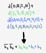
So, our final list of implicants is:
d(0,8,2,10)
d(5,7,13,15)
d(12,13,14,15)
d(2,3,10,11,6,14,7,15)
d(8,9,12,13,10,11,14,15)
We are almost done. Thanks for hanging in there.

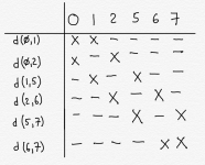
Here I’ve made a table with our implicants corresponding to rows, and the digits corresponding to columns. I’ve listed all the digits that correspond to a 1 or a d on the output of our truth table across the top. The box includes only the digits that need to produce a 1. Digits 10-15 are don’t cares. Remember that I said that our final solution has to cover all the 1’s and that we don’t care about the don’t cares. I’ve listed them for sake of completeness, but for the remaining steps we really don’t care about the columns outside the box.
Inside our table, I’ve placed an X under each digit if the corresponding implicant covers that digit. So, for example, d(0,8,2,10) covers digits 0, 2, 8 and 10, so I’ve placed X’s in those four positions.
Now, what we do next depends on our goal. This is where computer scientists and mathematicians have a bunch of algorithms for deciding which rows (which implicants) to include in the final solution. As a logic designer, however, our goal isn’t to optimize a single logic expression. Our goal is to optimize the chip. Before we get to that, however, let’s look at how the process would go if we only had to worry about generating this one logic expression.
First, we look at each column, one by one. If a column has only a single X in it, then we must include the implicant corresponding to that X. So, in this case, we notice that column 0 has only one X, corresponding to d(0,8,2,10). Therefore, d(0,8,2,10) will be in our final answer. We also see that column 3 has only a single X in it, so we must include d(2,3,10,11,6,14,7,15). And column 5 has only a single X, so we must include d(5,7,13,15). Finally, column 9 has only a single X in it, so we must include d(8,9,12,13,10,11,14,15).
Next, we pick rows that cover any columns we haven’t yet covered. We may want to pick the minimum number of rows that do the job, or we may have some other way of choosing; there are various algorithms for doing this, but in our case it is easy. That’s because the implicants we’ve already picked already cover all the columns up to column 9. We have no more work to do. Moreover, the only row that is left - d(12,13,14,15) - the one I added accidentally - couldn’t help us in any case. It has no X’s in columns up to 9.
So, our final answer is: d(0,8,2,10) + d(5,7,13,15) + d(2,3,10,11,6,14,7,15) + d(8,9,12,13,10,11,14,15)
Converting that to something useable to create logic, we look at the input bit patterns corresponding to each of those, and get:
-0-0 + -1-1 + --1- + 1---
(To see this yourself, just go back to our prior table that listed all the size-4 and size-8 implicants.)
Remember that each position in the bit patterns represents an input, in this order: b3 b2 b1 b0. The dashes represent don’t care states, the 0’s mean we need to invert the input, and the 1’s mean we do not invert the input. So, our logic expression is:
b2’ b0’ + b2 b0 + b1 + b3
Let’s check our work…

It works! We got the right answer, and the expression is a tiny bit simpler than what we got when we did the Karnaugh Map.
Remember that all of the work we’ve done so far is, unbelievably, just to develop a logic expression for controlling just one segment on a 7-segment LED. We would perform the same procedure to develop implicants for each of the other 7 segments. And we might find overlap. We might find, for example, that d(2,3,6,7) is on the list for two of the other segments. It was on our list of size-4 implicants but it didn’t make the final cut.
If we include the circuitry corresponding to d(2,3,6,7) in our design in order to deal with those other segments in the LED, we could make use of for segment A, as well, thus saving some power and die area. We had d(2,3,6,7) on our list of potential size-2 implicants, but it didn’t make the final list. Let’s go ahead and add it to our candidates and see where we stand.

This time I didn’t include any columns after digit 9, because, once again, we don’t care about those. We have added d(2,3,6,7) to our list, and we will declare that it must be included in the final result, because we want to take advantage of the fact that we already have the logic circuit that produces that term. Now we see that we do not need to include d(2,3,10,11,6,14,7,15). Both d(2,3,6,7) and d(2,3,10,11,6,14,7,15) have X’s in the same four columns, so including both of them would be redundant. The binary string corresponding to d(2,3,6,7) is 0-1-. That makes our new logic equation: b2’ b0’ + b2 b0 + b3 + b3’ b1. This is slightly more complex than our previous result, but the overall circuit design might end up simpler. (In this case, it’s not, but that’s a different story).
Just to double-check our results:
Once again, our work checks out.
Here are a few other similar properties:
(A)(0) = 0
A+0 = A
A+1 = 1
Here’s a more complicated one. A+AB = A
Let’s derive that:
This seems counterintuitive, but think of this example: Cat = feline + (feline AND orange)
Regardless of color, the feline is a cat. If feline is true, then we don‘t have to consider (feline AND orange), because the stand-alone feline term is enough to satisfy the expression. If feline is false, then both terms are false, so cat is false.
Here’s an even more complicated one: (A+B)(A+C) = A+BC
If A is true, then both A+B and A+C are true, so AND’ing them together is true. If A is false, then I need both B and C to be true so that when I AND them together, the result is true. A+BC is another way of expressing that - either A is true, or both B and C are true, in order for the expression to be true. I can derive this mathematically by treating the logic expression like normal math variables:

If we look at an example corresponding to variation (1), imagine the statement “I am neither a cat nor a dog.” The left side of expression one corresponds to that statement, if “I am a cat” is A and “I am a dog” is B. In that case, A+B would be “I am a cat or I am a dog.” And putting a line over A+B means “I am not a cat or a dog.” If I am neither a cat nor a dog, then I am not a cat and I am not a dog. That corresponds to the right side of the equation. So the equation makes sense based on our normal expectations for words like “nor” and “and.”
DeMorgan’s Law is important because it allows you to transform AND/NAND expressions into OR/NOR expressions, and vice versa. In a previous article, I explained that NANDs are preferred when creating CMOS logic circuits. A NAND function is the logical inversion of an AND function. NAND is true when at least one input is false. The truth table for a 2-input NAND is:

Looking back at the variations of DeMorgan’s Law, consider version (3). Put into words, what this equation says is that if I have an OR gate, I can convert it to a NAND gate simply by inverting each input. As a CPU designer I frequently used the various versions of DeMorgan’s Law (some complicated expressions require that you use more than one of the variations) to convert expressions to ”NAND form.”
Let’s see what we can do with the POS logic expression we derived using the Karnaugh Map.
We started with the AND of two ORs, and now we have the AND of two NANDs. One of the NANDs has 3-inputs and the other has 4. 3 isn’t ideal, but 4 is plain bad. we would probably break up the 4-input NAND (the second term) with two 2-input NAND gates connected to the inputs of a 2-input NOR (again, using DeMorgan’s Law). The AND of the two terms would probably be replaced with a NOR gate (using DeMorgan’s Law), but could be replaced with a NAND driving into an inverter; the latter makes more sense if we are driving a heavy capacitive load with this function.
In practice we may also split things into different sub-terms (probably 2-input) depending on what inverters we might already have available for use in other functions.
The first thing I notice is that when b3 is a 1, the output is always a 1. And when b1 is a 1, so, too, is the output. So if either b1 or b3 is a 1, the output is a 1. I know I can design logic like this to calculate this function: b1 + b3 + (some other cases where the output is 1). Notice that our solutions above took this form.
If I cross out the cases that are handled by b1 + b3, I am left with:

So I have two more rows to account for. When I compare them to the two rows that produce 0’s as outputs, I notice that one difference is that when the output is 1, b2 and b0 have the same value as each other, whereas when the output is 0, b2 and b0 have opposite values. So if I add these two terms to my equation, I capture the 1’s as outputs, but don’t accidentally capture the 0’s:
b2 b0
b2’ b0’
That means my final “in my head” expression would be: b1 + b3 + b2 b0 + b2’ b0’
That’s exactly what Quine McCluskey gave us, and it would take me, and most other logic designers, less than a minute to obtain that result.
Nonetheless, the tools I explained here are very important. Not all logic is so easy to analyze. And using software tools to find the answer isn’t always the best solution, because you may be optimizing for something different than the software tool.
Even if the details of how to do these calculations escapes you still, I hope you have gained a little bit of intuition about how there are many ways to create the same logic function, the importance of don’t cares, and the kinds of things that designers do to try and optimize things.
The easiest way to understand these techniques is to work through an actual problem. When I was but a wee undergrad engineering student, professor Jack Fitzgerald McDonald, in his hardware design class, gave us an assignment. Each of us was to design and build a functional electronic die. This consisted of some LEDs, representing each of the pips corresponding to a die face. There was also a button. Press and hold the button and the die face started flashing through different possible values very quickly. Release the button and the die stops and displays between 1 and 6 pips. To do this I used a 555-timer chip, a bunch of logic gate chips, a couple of NAND gates to de-bounce the push button, and a lot of little wires.
We’ll use that as inspiration for a slightly different problem, addressing a 7-segment LED.
These things are (or used to be) ubiquitous. Every clock radio, digital clock, lots of signs, etc. use variations of this thing. Above we have a 7-segment LED, with an 8th element (a decimal point). The segments are labeled from A to G.
Depending on what number you are displaying, different segments are turned on. Let’s look at segment A. It is lit up for some, but not all, digits:
From the image above, we see that segment A is lit up for the following digits: 0, 2, 3, 5, 6, 7, 8 and 9. It is not lit up for digits 1 and 4.
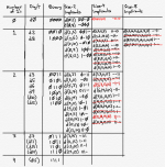
Truth Tables
Now, imagine that we have a binary counter that can output, in sequence, integer values, starting at 0. The decimal value and the corresponding binary equivalent are shown below, in the form of a truth table:
The way this table is read is that inputs to the logic function are on the left (here the decimal value is in the leftmost column and the binary equivalent is in the middle column) and outputs are in the right column.
We only care about the digits 0 through 9, because that’s all you can display in a single 7-segment LED. The counter will have four output wires: b3, b2, b1, b0. We will assume that the digit we want to display on the 7-segment LED will correspond to the decimal value corresponding to those four wires arranged in that order. (This mapping is arbitrary. If I wanted to, I could have the LED display 4 when the counter outputs 6, or whatever. In some cases, rearranging things in such a way can be useful; it may reduce circuit noise or power consumption, or the number of gates required. This is something else that logic designers must consider, but I don’t want to bite off more than we can chew in this article).
Don’t Cares
Note that we have four output wires from the counter, which means we can have 16 possible output values, but we are only using 10 of them. We don’t care about the remaining values. Don’t care is a wonderful term-of-art in logic design. It means that for certain combinations of input values, we really don’t care what the output is. This means that we don’t have to work hard to try to make those outputs have any particulate value when those input combinations are active, freeing us from having to include yet more logic to address those combinations. Often times we use the symbol “d” or it’s greek equivalent to represent don’t care in truth tables and when working with logic equations.
I can’t emphasize enough how excited I get by don’t cares. Many times I have run into thorny problems meeting my timing goals and found that I could solve the problem by realizing that there were don’t cares that the architect didn’t notice (or chose to ignore). What happens is that the architect who writes the high level behavioral model for the chip can easily write smaller logic equations by ignoring don’t cares. If some combination of inputs is impossible, for example, it is easier to just ignore that possibility when writing the architectural model than it is to specifically call that out by making the logic more complicated and treating the don’t cares separately. Often times I would stare at the logic for a long time and realize there were hidden don’t cares that I could take advantage of.
Above, I have augmented the table to add don’t cares. We are going to use the heck out of those.
Karnaugh Maps
The first technique taught to fledgling logic monkeys is the Karnaugh Map. The Karnaugh Map is a useful logic minimization technique as long as you have three or four inputs. It’s possible to use with five or six inputs, and I’ve done it a few times, but it’s not a lot of fun; it’s literally a bit like 3D chess in that case.
We have four inputs - b3, b2, b1, and b0 - so we are good to go with a Karnaugh Map.
Above is the Karnaugh Map for our problem. Along the left side are b3 and b2 and along the top are b1 and b0. So, for example, if we are looking for the case where b3 b2 b1 b0 = 1101, then that is the third row down (where b3 b2 = 11) and the second column from the left (where b1 b0 = 01).
Inside each square, we put a 0, a 1, or a d, depending on the value from our truth table (the right-most column from the tables at the top of this article).
Note that the rows and columns proceed in a funny order. Normally, when counting in binary, we would count like this: 00, 01, 10, 11. Here we are counting 00, 01, 11, 10. This type of counting, called Gray coding, has fun properties that help the Karnaugh Map work. The idea is that each neighbor differs by only 1 digit. That also includes when we wrap around - 00 differs from 01 by one digit, but it also differs from 10 by one digit.
There are two ways to use a Karnaugh Map - it can be used to produce what is called a “Sum of Products” or to produce a “Product of Sums” (SOP or POS, respectively). For some reason, young logic designers seem to always prefer SOP, so we’ll start there.
Sum of Products
To find the SOP form from a Karnaugh Map, we try to find the biggest rectangle we can that contains only 1’s. The quantity of squares in the rectangle must be a power-of-2. In other words, the rectangle we identify must have 16, 8, 4, 2, or 1 squares in it. Since we want to find a big rectangle, we treat the d’s as if they are 1’s - that improves the likelihood that we can make a bigger rectangle. Note that you can wrap around when finding the rectangle. That is, you can start in the fourth column and then include squares from the first column. We will have an example of that in a bit.
We have a couple of choices for the biggest rectangle containing only 1’s and d’s, so below I have picked one:
Here I’ve drawn a red rectangle containing 8 squares. 8 is a power of 2, so that works. I can’t make the rectangle any bigger without including a 0, and that would be illegal. I could have, instead, drawn a rectangle around the bottom two rows. In the end, this choice doesn’t matter, because both options include 8 squares.
Next I repeat the process, until all of the 1’s in the Karnaugh Map exist inside a rectangle. I don’t have to include all the d’s, but whenever convenient I can treat d’s as 1’s.
Below I’ve drawn the next biggest rectangle I can draw that includes 1’s that were not already captured by a rectangle. I did this with the blue rectangle:
Note that my rectangles overlap. That’s perfectly fine. At this point I have two more 1’s, at the top left, that are not yet in rectangles. So I keep going.
This time I‘ve draw a green square. That sucked in one of those rogue 1’s. The square covers four entries In the map, and 4 is a power of 2. That’s why I couldn’t extend the square to the right or down to include more 1’s (or d’s). That would result in a rectangle covering 6 squares, and 6 is not a power of 2. And I can’t extend the bottom right corner of the green square to the bottom right corner of the map, because then I would have 9 entries in my square, and 9 is not a power of 2.
I now have one more 1 left to capture:
Now I am done. I have no more 1’s left to capture. Usually, at that point, I’d head across the street from AMD and get a burrito. But I assume you already have a burrito, so we’ll move on to our next steps.
What we need to do is look at one rectangle at a time, and for that rectangle, figure out what values of b3, b2, b1, and b0 do not change. Pay close attention here and you’ll get it, no problem.
Let’s start with the yellow rectangle. The yellow rectangle covers these two values of b3 b2 b1 b0: 0000 and 0010. You can tell simply by reading the values of the left and top sides of the Karnaugh Map. The top left square is at b3 b2 = 00 and b1b0 = 00 (concatenating those gives 0000). The top right square is at b3 b2 = 00 and b1 b0 = 10 (giving us 0010).
So we have two values: 0000 and 0010. Which digits are identical between those two values? These: 00-0. The first, second and last. The third digit does change - it’s a 0 in the left square and a 1 in the right square. The digits that match each other correspond to b3, b2, and b0. As a result, we can extract a “product” (remember: we are doing “sum of products”) corresponding to b3, b2 and b0 and ignoring b1. Since the digits are 0’s, and we are doing SOP form, we need to invert b3 b2 and b0. If the digits were 1’s, we wouldn’t invert. If the digits were 0’s but we were doing POS, we wouldn’t invert (but we would also be covering 0’s, not 1’s, with our rectangles).
That means that the product, or min term (Boolean math has some crazy nomenclature), corresponding to the yellow rectangle is b3’ b2’ b0’. These are written without any operator between them, like you’d write multiplication of variables in algebra - hence the name “product.” The apostrophe after each variable is a way of saying “the inversion of this variable.” We would read this as “b3 prime” or “not b3,” depending on preference. Logic designers have way too many ways of indicating inversion - apostrophes, lines over the variable, prefacing or suffixing with exclamation points, prefacing with a tilde… Sorry about that.
The implied operator is the Boolean AND function. What we are saying is that if we AND together b3’, b2’ and b0’ and get a 1, then the LED segment should be lit up. In other words, if b3’, b2’ AND b0’ are all 1’s, then the segment is lit. Which is another way of saying that b3, b2 and b0 all being 0’s means the segment is lit; because b3 is the opposite of b3’, b2 is the opposite of b2’ and b0 is the opposite of b0’.
Note that if any of the products evaluates to true (i.e. a 1), then the segment lights up. And each product corresponds to one of our rectangles.
To save you from scrolling, here’s our Karnaugh Map again. Let’s look at the green square. It corresponds to four values of b3 b2 b1 b0: 0101, 0111, 1101, and 1111. We need to identify which digits of those four values are identical across all four values. The left-most digit, corresponding to b3, is sometimes a 0 and sometimes a 1. So we ignore that. The next digit, corresponding to b2, is always a 1. So we keep that. The next digit, corresponding to b1, is sometimes a 0 and sometimes a 1, so we ignore that. And the right-most digit, corresponding to b0, is always a 1, so now we know that our answer will involve b2 and b0, because those two bit positions never change. We also see that each is always a 1. Since we are doing SOP and these are 1’s, we do not have to invert. That means that our second product, which corresponds to the green square, is b2 b0. If b2 and b0 are both 1’s, then our LED segment should turn on.
Note that we have a pattern developing. Our first rectangle had 2 entries in it, and produced a product with 3 variables in it. Our second rectangle had 4 entries in it, but produced a product with only 2 variables in it. So far it looks like maybe the bigger the rectangle, the smaller the product. Smaller products require less logic - fewer transistors and less power consumption - to implement.
The remaining two rectangles each cover 8 entries. Let’s do the blue one.
Here are the values of b3 b2 b1 b0 that are covered by the blue rectangle:
b3 | b2 | b1 | b0 |
1 | 1 | 0 | 0 |
1 | 1 | 0 | 1 |
1 | 1 | 1 | 1 |
1 | 1 | 1 | 0 |
1 | 0 | 0 | 0 |
1 | 0 | 0 | 1 |
1 | 0 | 1 | 1 |
1 | 0 | 1 | 0 |
There is only one column where the value doesn’t change: b3. Since the value in that column is always a 1 and we are doing SOP, then our product is simply b3. If b3 is a 1, then our segment should light up.
Finally our red rectangle. I‘ll leave this as an exercise for the reader to prove, but the only input that doesn’t change is b1, which is always 1. So if b1 is a 1, then our segment should light up.
What we do next is we write out our sum of the four products we just found:
We’ve just written a “sum of products,” reduced form of the logic equation that gives us the truth table we started with. The “+” operator means ”Boolean OR.” (As usual, there are many ways to write an “OR,” including a ”v,” a “|,” and probably a bunch of other symbols that aren’t currently coming to mind. (Logic designers borrow from many disciplines, including math, physics, computer science, etc. We end up being fluent enough in all of them that we mix and match terminology in ways that would give a pure mathematician or a pure computer scientist heartburn).
This equation may seem fairly complicated, but let’s compare that to the naive SOP representation that we can automatically derive from the original truth table - to do that, we simply sum up the products that correspond to each row that has a 1 in its output column:
In the above truth table, I’ve added two new sections. Remember, for the minimized logic equation to be correct, it must produce the same values as are shown in the red column. It must produce a 1 whenever the LED segment should be lit, and a 0 otherwise. We don’t care what results we get for the rows that are marked “d,” because these are don’t cares.
In the first new section, I added a column for each of the four products in our sum of products. The first column is simply b1. The second column is b3. The third column is the product b2 b0. The “product” is produced by performing the Boolean AND function; this means it produces a 1 only when both b2 and b0 are 1’s. Otherwise it produces a 0.
The fourth column corresponds to the final term, b3’ b2’ b0’. This produces a 1 only when b3, b2 and b0 are 0 (because we need to invert each value before we perform the Boolean AND).
The right-most section of the above table is the “sum” of the four products. This “sum” is really a Boolean OR operation; it means that the result is a 1 only if any of the four products is a 1. You can see from the blue column that the answer is correct; it matches the red column perfectly (if we ignore the “d” entries).
Comedy from Errors
I intentionally made a mistake above. Did you catch it? I did It to make our analysis more interesting, but as a result of this mistake, the answer is not actually the smallest expression that we could obtain. So let’s fix the mistake and try again.
If you look at the yellow rectangle, you will remember that I wrapped off the left and right sides of the map. But I can also wrap off the top and bottom! That would give us the following Karnaugh Map:
Now our yellow rectangle is a square that covers the four corners of our Karnaugh Map. That means we need to revisit the product corresponding to the yellow rectangle. What stays constant in those four yellow squares? In all four, b2 is 0. And in all four, b0 is 0. So, the term would be b2’ b0’.
That means, our corrected sum of products from this Karnaugh Map is: b1 + b3 + b2 b0 + b2’ b0’. That’s a little simpler, because we were able to make one of our rectangles a little bigger. We are going to prove that this logic expression is correct later on in this article, when we arrive at the same solution using a completely different method.
Product of Sums
The Sum of Products is the logical OR of a bunch of terms, each of which is a logical AND. In earlier articles in this series, I explained why positive logic functions like AND and OR should be avoided when designing CMOS logic circuits, when possible. It’s possible to convert a logic equation in SOP form into NAND logic, but it’s a bit easier to do so from Product of Sum (POS) form. To be clear, in neither case is it easy; it takes some expertise to do this transformation whether you are starting from POS or SOP form. This is particularly the case if you are trying to optimize the equation so that it relies mostly on 2-input gates (which are much better than 3-input or higher-input gates) and mostly relies on NANDs with a minimum number of additional inverters. We’ll save most of that for our advanced course.That said, let’s look at how you do a Karnaugh Map to produce a POS expression.
First, here’s our Karnaugh Map again:
This time we are going to produce rectangles that cover the 0’s, and not the 1’s. We can treat the d’s as 0’s to make it possible to make larger rectangles. This time our rectangles won’t be able to be so big. The biggest rectangle we can make is the red rectangle below, which covers b3 b2 b1 b1 = 0100 and 1100.
We learned earlier that bigger rectangles make for shorter terms (in this case instead of products, we have sums. And the sums are sometimes called maxterms. Because, once again, logic designers like to use all the nomenclature they can find.). The don’t cares help us in this case; otherwise we would have no rectangle bigger than a single entry.
We still have one more 0 to cover. That’s done below with the nice blue square.
Now we will look at one rectangle at a time and extract a sum for each. This time, we invert if the corresponding bits in the inputs are 1’s, instead of 0’s.
Looking at the red rectangle, we said our entries corresponded to 0100 and 1100. The first bit differs between the two, but b2, b1 and b0 are the same. So these bits will be part of our sum. We need to invert b2, because in both entries b2 is a 1. So, our first sum is b2’ + b1 + b0.
For the blue square, we end up with b3 + b2 + b1 + b0’ (I’ll leave that as an exercise for the reader).
Our overall product of sums, therefore, is (b2’ + b1 + b0)(b3 + b2 + b1 + b0’).
The following truth table tests our result.
Each of the two sums has its own column. Remember that a “sum” is the logical OR of its terms. Meaning that the result is 1 if any of the terms (taking into account any indicated inversions) is a 1. The final answer, the “product” (which is the logical AND of the two sums) is shown in the right-most column. If we ignore the don’t cares (as we should), the results perfectly match the desired results (shown in the Segment A column).
Different Quantities of Inputs
All of our examples involved Karnaugh Maps with 4 inputs: b3, b2, b1 and b0. A 3-input Karnaugh Map is handled the same way, and looks like this:If we have 5 or 6 inputs, we need to go in 3-dimensions, like 3D chess:
Here I’ve shown a partial 5-input Karnaugh Map. I have two 4-input Karnaugh Maps, that are tied together. One of the two corresponds to when b4=0 and the other corresponds to when b4=1. I’ve shown a red and blue square/rectangle that span across the two maps. The green rectangle is found on only one of the two maps, corresponding to b4=1. I also indicated the minterms (the products) corresponding to each; I’ll leave their derivation to the reader.
If I have 6 inputs, I would stack four maps, each corresponding to a pair of values for the 5th and 6th board. I could keep going, but then I‘d need to think in four dimensions or more. It quickly gets to the point where using a Karnaugh Map becomes impractical. Which brings us to the next technique.
Quine-McCluskey Method
The Quine-McCluskey Method is considerably less graphical and less fun than Karnaugh Maps, but is much more scalable to high numbers of inputs. It’s also readily implemented using computer algorithms. It does require a bunch of steps and you have to be careful with your bookkeeping, however.We start by looking at our truth table again. We will only pay attention to rows where the output is a 1 or a don’t care (hence the red lines through the two rows where the output is a 0).
We are going to look at the inputs corresponding to each row that remains after we cross out the 0-rows, and count how many 1’s there are. For example, the first row, corresponding to digit 0, has no 1’s among b3, b2, b1 or b0. The row corresponding to digit 2 has a single 1 (corresponding to b1). Etc. We are going to group the rows together based on how many 1’s are in the inputs for each row, as follows:
The left column is how many 1’s are in the inputs in that group. The middle column is shorthand for each row from the truth table: d0 means the row for digit 0, and d8 means the row for digit 8, for example. If the row was a don’t care row, I put it in parentheses (just to keep track of it). The right column is the set of inputs (b3 b2 b1 b0) corresponding to that digit/row. So, for example, in our truth table we saw that we had a row for digit 8, which corresponded to the set of inputs 1000. There is a single 1 in that set of inputs. So in the table, in group 1 (corresponding to a single 1 in the inputs), we have d8 and 1000.
This grouping isn’t strictly necessary, but it makes the algorithm a little easier to do when you are doing it by hand; as you’ll see, in subsequent steps it means we only have to work in one direction - downward - which makes things less confusing.
Our next step will be to find what are called implicants. These are sort of like the rectangles we found in the Karnaugh Maps, but not quite. We will repeat the search for implicants in stages. First we will find “size 2” implicants, then “size 4,” then ”size 8,” etc. We stop when we can’t go any further.
So, how do we find size 2 implicants? We walk through the table above, looking at our binary inputs, and finding rows that match except for exactly one difference. Let’s do some examples.
Let’s start with d0, which corresponds to 0000. We start going downward, row-by-row, until we find a binary string that differs in only one position. So, for example, d2, which is 0010, differs from 0000 in only one position. We therefore can combine these two entries into a size-2 implicants, which we can write as d(0,2) and the binary string 00-0 (or 00d0, or 00x0, or whatever nomenclature makes you happy). The dash (“-”) goes in the bit position that has a different value between d0 and d2.
Now we keep going, looking for more rows we can combine with d0. It turns out that d8 is 1000, so we can create an implicants d(0,8) with binary string -000. We put the dash in the first position because d0 has a 0 in that position and d8 has a 1 in that position.
At this point we can stop looking for things to combine with d0. Remember that you must have one and only one difference between the rows we are combining. Since d0 has no 1’s in it, and d2 and d8 have a single 1 in them, we can combine them. But anything from the subsequent groups will have at least two 1’s in the binary strings. Going from all 0’s to a string with two 1’s in it means at least two bit positions must differ, which means we can’t combine.
So far we have this:
We’ve created a new column for the size-2 implicants. We found two such implicants, both involving d0 on the one hand and an entry from the “1” group from our previous table on the other hand.
Returning to our prior table, next we look at d2, which corresponds to binary string 0010. Because we organized our table Into groups based on the number of 1’s in the binary strings, we only have to look down the table, and don’t have to look at group 0 anymore.
We can’t combine d2 (0010) with d8 (1000) because there are two bits that differ between those binary strings; the first bit and the third bit. So we keep looking downward, in group 2.
d3 (0011) differs from d2 (0010) in only one bit position - the rightmost one. We can create an implicant d(2,3) with pattern 001- by combining d2 and d3.
If we keep going, we’ll see that d2 (0010) and d5 (0101) differ in 3 positions, so we can’t combine them. We can, however, combine d2 (0010) with d6 (0110) to create d(2,6) (0-10). We‘ll also find that d(2,10) works, which I’ll leave to the reader to prove.
Once we run out of things to combine with d2, we look at d8. Below, I’ve written the implicants that correspond to group 0 and group 1. Feel free to double-check my work.
We keep doing this, going group-by-group and row-by-row, until we reach the bottom. This gives us the following table:
You can already see why this is a lot more tedious than Karnaugh Maps, at least for four inputs, and we’re not close to done yet.
Next we are going to find size-4 implicants. Finding size-4 implicants is similar to finding size-2 implicants, but instead of looking at our original binary column, we look at the binary patterns in the size-2 implicants column. We treat dashes as “must match.” So, for example, we could combine 110- and 100- because they have a dash in the same (rightmost) bit position, and there is only 1 difference in the remaining bit positions (the second bit from the left). We would therefore combine 110- and 100- into 1-0-, placing a second dash in the bit position where there is a difference between the binary strings.
So, let’s start at the top of our list of size-2 implicants:
d(0,2) has a dash in the third position. We can only combine it with other size-2 implicants that also have a dash in the third position. Look downward through our list, the first possibility is d(5,7):
I’ve put red boxes around each size-2 implicant with a dash in the third position; all of them have at least two 1’s, but d(0,2) has no 1’s. This means that all of them differ from d(0,2) in at least 2 bit positions. So, looking at d(5,7) (01-1) and comparing it to d(0,2) (00-0), we see that the rightmost bit differs, and so does the second bit from the left. Therefore these cannot be combined. The same is true of all the other candidates. Therefore d(0,2) cannot be part of a size-4 implicant, and we move on to d(0,8).
This time I’ve cropped our table to only show up through group 1; the groups below group 1 will have at least two 1’s in every entry, and d(0,8) has zero 1’s. We need a single 1 otherwise more than one bit position will differ from d(0,8).
d(2,10) is our only candidate in group 1. d(0,8) (-000) differs from d(2,10) (-010) only in a single position - the second from the right. As a result we can combine these two size-2 implicants into a size-4 implicants: d(0,8,2,10) which has bit pattern -0-0. The second dash is because d(0,8) has a 0 in that position whereas d(2,10) has a 1.
This also means we have accounted for d0, d2, d8, and d10 from our list of digits (In the second column of our table). By the time we are done, we need to have accounted for every digit that corresponds to a 1 on the output: 0, 2, 3, 5, 6, 7, 8, 9. We don’t care about the aptly-named don’t cares. So, in other words, in the “Digit” column of our grouped table, we care about each Digit that is not in parentheses. I bring this up now because, recall, d(0,2) couldn’t be combined with anything. Once we run out of combinations we can make, we need to decide which implicants make our final list. Our list could have some size-8 implicants, some size-4 implicants, and some size-2 implicants, for example. If d0 or d2 is not found in a big implicant (a size-4 or size-8, say), then we would have to include d(0,2) in our final list of implicants, even though it is a puny size-2 implicant.
In any event, we continue this process, moving on to d(2,3), then d(2,6), etc. We find as many size-4 implicants as we can. Then we go through each size-4 implicant and try to combine them to create size-8 implicants. Then we try to make size-16 implicants. This is the point where I pull the finished pot roast from the oven and skip over an hour’s worth of work:
As you can see, we have some size-8 implicants, but we can go no further; none of the size-8 implicants can be combined. There are a couple more things to note.
First, you will notice that some implicants have a red line through them. These are duplicates - they are the same as other implicants, just with the list of digits in a different order. If I was doing this exercise for real and not for explaining to others, each time I created an implicant I would sort the list of digits. So d(0,8,2,10) would be d(0,2,8,10). The order doesn’t matter. Sorting helps identify duplicates and makes it easier to keep track of which digits I have managed to cover. The downside is it makes it harder to keep track of what I combined in order to make the bigger implicants.
In any event, we can ignore the duplicates; regardless of the order of the digits in the implicants, the bit patterns will be the same.
Second, you will see that some of the size-4 implicants are written in red. Earlier I mentioned that we may need to include smaller implicants in our final list, if they cover digits that the bigger implicants don’t cover. That’s what the red implicants are. For example, d(0,8,2,10) is in red. If you look at the size-8 implicants, you can see that none of them cover digit 0. In order to include digit 0 in our final answer, therefore, we need to include d(0,8,2,10), a size-4 implicant. Similarly, d(5,7,13,15) is required in order to cover digit 5.
d(12,13,14,15) is a different story. It’s in red because… I made a mistake. But rather than fix my mistake, I decided to go with it, to illustrate how the next step will automatically correct my error.
So, our final list of implicants is:
d(0,8,2,10)
d(5,7,13,15)
d(12,13,14,15)
d(2,3,10,11,6,14,7,15)
d(8,9,12,13,10,11,14,15)
We are almost done. Thanks for hanging in there.
Here I’ve made a table with our implicants corresponding to rows, and the digits corresponding to columns. I’ve listed all the digits that correspond to a 1 or a d on the output of our truth table across the top. The box includes only the digits that need to produce a 1. Digits 10-15 are don’t cares. Remember that I said that our final solution has to cover all the 1’s and that we don’t care about the don’t cares. I’ve listed them for sake of completeness, but for the remaining steps we really don’t care about the columns outside the box.
Inside our table, I’ve placed an X under each digit if the corresponding implicant covers that digit. So, for example, d(0,8,2,10) covers digits 0, 2, 8 and 10, so I’ve placed X’s in those four positions.
Now, what we do next depends on our goal. This is where computer scientists and mathematicians have a bunch of algorithms for deciding which rows (which implicants) to include in the final solution. As a logic designer, however, our goal isn’t to optimize a single logic expression. Our goal is to optimize the chip. Before we get to that, however, let’s look at how the process would go if we only had to worry about generating this one logic expression.
First, we look at each column, one by one. If a column has only a single X in it, then we must include the implicant corresponding to that X. So, in this case, we notice that column 0 has only one X, corresponding to d(0,8,2,10). Therefore, d(0,8,2,10) will be in our final answer. We also see that column 3 has only a single X in it, so we must include d(2,3,10,11,6,14,7,15). And column 5 has only a single X, so we must include d(5,7,13,15). Finally, column 9 has only a single X in it, so we must include d(8,9,12,13,10,11,14,15).
Next, we pick rows that cover any columns we haven’t yet covered. We may want to pick the minimum number of rows that do the job, or we may have some other way of choosing; there are various algorithms for doing this, but in our case it is easy. That’s because the implicants we’ve already picked already cover all the columns up to column 9. We have no more work to do. Moreover, the only row that is left - d(12,13,14,15) - the one I added accidentally - couldn’t help us in any case. It has no X’s in columns up to 9.
So, our final answer is: d(0,8,2,10) + d(5,7,13,15) + d(2,3,10,11,6,14,7,15) + d(8,9,12,13,10,11,14,15)
Converting that to something useable to create logic, we look at the input bit patterns corresponding to each of those, and get:
-0-0 + -1-1 + --1- + 1---
(To see this yourself, just go back to our prior table that listed all the size-4 and size-8 implicants.)
Remember that each position in the bit patterns represents an input, in this order: b3 b2 b1 b0. The dashes represent don’t care states, the 0’s mean we need to invert the input, and the 1’s mean we do not invert the input. So, our logic expression is:
b2’ b0’ + b2 b0 + b1 + b3
Let’s check our work…
It works! We got the right answer, and the expression is a tiny bit simpler than what we got when we did the Karnaugh Map.
Remember that all of the work we’ve done so far is, unbelievably, just to develop a logic expression for controlling just one segment on a 7-segment LED. We would perform the same procedure to develop implicants for each of the other 7 segments. And we might find overlap. We might find, for example, that d(2,3,6,7) is on the list for two of the other segments. It was on our list of size-4 implicants but it didn’t make the final cut.
If we include the circuitry corresponding to d(2,3,6,7) in our design in order to deal with those other segments in the LED, we could make use of for segment A, as well, thus saving some power and die area. We had d(2,3,6,7) on our list of potential size-2 implicants, but it didn’t make the final list. Let’s go ahead and add it to our candidates and see where we stand.
This time I didn’t include any columns after digit 9, because, once again, we don’t care about those. We have added d(2,3,6,7) to our list, and we will declare that it must be included in the final result, because we want to take advantage of the fact that we already have the logic circuit that produces that term. Now we see that we do not need to include d(2,3,10,11,6,14,7,15). Both d(2,3,6,7) and d(2,3,10,11,6,14,7,15) have X’s in the same four columns, so including both of them would be redundant. The binary string corresponding to d(2,3,6,7) is 0-1-. That makes our new logic equation: b2’ b0’ + b2 b0 + b3 + b3’ b1. This is slightly more complex than our previous result, but the overall circuit design might end up simpler. (In this case, it’s not, but that’s a different story).
Just to double-check our results:
Once again, our work checks out.
Some Other Logic Tricks
When manipulating logic expressions, you can often treat them as if AND is multiplication and OR is addition, especially if you assume the variables can only have two different values: 0 (false) or 1 (true). That gives rise to some fun tricks.(A)(A) = A
If you AND any value with itself, you get that value. A x A is A, not A squared. That makes sense if you consider that A can only be a 0 or a 1. If A is a 1, then AxA = 1, which is A. If A is a 0, the AxA = 0, which is A.(A)(1) = A
If you AND any value with 1, you get that value. This makes sense if you treat AND as multiplication. And it makes sense if you consider that A can only be 1 or 0. If A is 1, then ANDing it with 1 is 1, which is A. And if A is 0, then ANDing it with 0 is 0, which is A.A+A = A
If you OR anything with itself, you just get that thing. OR is true if either input is true, otherwise it is false. ORing something with itself will result in both inputs being 0’s or both inputs being 1’s.Other Simple Properties
Here are a few other similar properties:
(A)(0) = 0
A+0 = A
A+1 = 1
Here’s a more complicated one. A+AB = A
Let’s derive that:
Code:
A+AB
A(1+B)          // factor out A
A(1)           // OR’ing something with 1 is 1
A          // AND’ing something with 1 is that thing
This seems counterintuitive, but think of this example: Cat = feline + (feline AND orange)
Regardless of color, the feline is a cat. If feline is true, then we don‘t have to consider (feline AND orange), because the stand-alone feline term is enough to satisfy the expression. If feline is false, then both terms are false, so cat is false.
Here’s an even more complicated one: (A+B)(A+C) = A+BC
If A is true, then both A+B and A+C are true, so AND’ing them together is true. If A is false, then I need both B and C to be true so that when I AND them together, the result is true. A+BC is another way of expressing that - either A is true, or both B and C are true, in order for the expression to be true. I can derive this mathematically by treating the logic expression like normal math variables:
Code:
(A+B)(A+C) = (A)(A)+(A)(C)+(B)(A)+(B)(C)  // multiply the two terms
           = A + AC + BA + BC             // (A)(A) = A; A can either be 0 (false) or 1 (true)
           = A(1+C) + B(A+C)              // factor
           = A(1) + B(A+C)               // Anything OR’d with TRUE (1) is just TRUE
           = A + B(A+C)                  // “A“ AND’d with TRUE is just ”A”
           = A + BA + BC                 // Multiply
           = A(1+B) + BC                 // Factor
           = A(1) + BC                  // Anything OR’d with TRUE (1) is just TRUE
           = A + BC                      // “A“ AND’d with TRUE is just ”A”
DeMorgan’s Law
One of the most important logical tricks is DeMorgan’s Law, which is a law I’ve mentioned in a previous article. There are numerous ways to write DeMorgan’s Law - here are a few:If we look at an example corresponding to variation (1), imagine the statement “I am neither a cat nor a dog.” The left side of expression one corresponds to that statement, if “I am a cat” is A and “I am a dog” is B. In that case, A+B would be “I am a cat or I am a dog.” And putting a line over A+B means “I am not a cat or a dog.” If I am neither a cat nor a dog, then I am not a cat and I am not a dog. That corresponds to the right side of the equation. So the equation makes sense based on our normal expectations for words like “nor” and “and.”
DeMorgan’s Law is important because it allows you to transform AND/NAND expressions into OR/NOR expressions, and vice versa. In a previous article, I explained that NANDs are preferred when creating CMOS logic circuits. A NAND function is the logical inversion of an AND function. NAND is true when at least one input is false. The truth table for a 2-input NAND is:
Looking back at the variations of DeMorgan’s Law, consider version (3). Put into words, what this equation says is that if I have an OR gate, I can convert it to a NAND gate simply by inverting each input. As a CPU designer I frequently used the various versions of DeMorgan’s Law (some complicated expressions require that you use more than one of the variations) to convert expressions to ”NAND form.”
Let’s see what we can do with the POS logic expression we derived using the Karnaugh Map.
Code:
(b2’ + b1 + b0)(b3 + b2 + b1 + b0’)    // The POS expression form the Karnaugh Map
!(b2 b1’ b0’) (b3 + b2 + b1 + b0’)     // Convert the first OR term to a 3-input NAND using (2)
!(b2 b1’ b0’) !(b3’ b2’ b1’ b0)       // Convert the second OR term using (2)
We started with the AND of two ORs, and now we have the AND of two NANDs. One of the NANDs has 3-inputs and the other has 4. 3 isn’t ideal, but 4 is plain bad. we would probably break up the 4-input NAND (the second term) with two 2-input NAND gates connected to the inputs of a 2-input NOR (again, using DeMorgan’s Law). The AND of the two terms would probably be replaced with a NOR gate (using DeMorgan’s Law), but could be replaced with a NAND driving into an inverter; the latter makes more sense if we are driving a heavy capacitive load with this function.
In practice we may also split things into different sub-terms (probably 2-input) depending on what inverters we might already have available for use in other functions.
Wrap Up
We’ve done an awfully large amount of work and we’ve managed to find several ways to design the logic to control one out of seven segments in our 7-segment LED. It would be natural to ask if this is how I would really do such a task. Well, the answer is yes and no. First, I made more tables and showed more intermediate work than I ordinarily would have. And I would often use automated tools to do some of this type of work. However, I did very often use of Karnaugh Maps and Quine McCluskey, scribbling things down on scrap paper, to simplify complex logic equations and get a feel for the potential set of individual minterms or maxterms I might be able to use in my design. And, quite often, I would simply do a lot of the simplification in my head. Let’s return to our original truth table for a moment:The first thing I notice is that when b3 is a 1, the output is always a 1. And when b1 is a 1, so, too, is the output. So if either b1 or b3 is a 1, the output is a 1. I know I can design logic like this to calculate this function: b1 + b3 + (some other cases where the output is 1). Notice that our solutions above took this form.
If I cross out the cases that are handled by b1 + b3, I am left with:
So I have two more rows to account for. When I compare them to the two rows that produce 0’s as outputs, I notice that one difference is that when the output is 1, b2 and b0 have the same value as each other, whereas when the output is 0, b2 and b0 have opposite values. So if I add these two terms to my equation, I capture the 1’s as outputs, but don’t accidentally capture the 0’s:
b2 b0
b2’ b0’
That means my final “in my head” expression would be: b1 + b3 + b2 b0 + b2’ b0’
That’s exactly what Quine McCluskey gave us, and it would take me, and most other logic designers, less than a minute to obtain that result.
Nonetheless, the tools I explained here are very important. Not all logic is so easy to analyze. And using software tools to find the answer isn’t always the best solution, because you may be optimizing for something different than the software tool.
Even if the details of how to do these calculations escapes you still, I hope you have gained a little bit of intuition about how there are many ways to create the same logic function, the importance of don’t cares, and the kinds of things that designers do to try and optimize things.