In Part 1, we discussed how the architect decides how the processor behaves. The next step is for the logic designer to decide how to produce that behavior. When I use the term “logic design,” I use it the way it was used at the various companies I worked at (AMD, Sun, Exponential Technology) and other companies where I was offered logic design jobs. Other companies, designing things like GPUs, ASICs, etc., have a very different view of how logic design is done. And logic design has, over the years, evolved to be more automated as the number of transistors in designs grow.
The logic designer is responsible for producing an actual design that behaves in the way the architects intended. This involves designing logic circuits, figuring out how to physically implement the logic circuits, and making sure the circuits meet various constraints (including timing, power, area, and other electrical issues).
The standard-cell blocks are created by arraying a set of “standard cells,” each of which corresponds to one or more logic gates, much like one builds a house out of Lego bricks. The individual cells usually correspond to simple logic functions, seldom with more than 5 or 6 inputs and 1 or 2 outputs, and most standard cells have just two or three inputs and one output. Standard cells usually have names like NAND2x1, NAND2x2, and INVx4. The logic function is indicated by the start of the name, the number of inputs comes before the “x,” and the number after the “x” is the strength of the gate (corresponding to the relative size of its transistors).

Example standard cell dimensions from a TSMC standard cell library
Typically, each standard cell has the same height, so that they can be arrayed in rows, but the width of standard cells may vary. A power rail and a ground rail are found at the top and bottom of each cell, so that when the cells abit a complete horizontal power rail and ground rail is formed.
At the companies I worked at, we designed the standard cells ourselves. This involved creating circuit diagrams for each cell, laying out the cell (i.e. generating the necessary polygons on each layer), and characterizing the electrical behavior of each cell. Companies may also use standard cell libraries provided by whatever fab they are using.
The process used to generate standard cell-based designs is iterative. The following loop is performed until all timing and electrical requirements are achieved.

Floor plan for the Exponential x704
These constraints include:
Below I’ll walk through some of the factors that a high-end CPU designer considers when performing design work.
Consider an inverter, the simplest CMOS logic gate. An inverter simply produces, as its output, the opposite logic value of its input. A rising voltage on the input of an inverter, for example, produces a falling output on the output of the inverter. In the above figure, the inverter has input A and output Z. The top graph shows a rising edge on the input of the inverter. As shown in the bottom graph, this produces a falling edge on the output of the inverter.
From the perspective of a logic designer, there are multiple considerations here. We need to understand the timing relationship between the waveform on the input and the waveform on the output. The way this is typically modelled is by defining two relevant timing characteristics. The first is the delay from the input to the output, indicated above as Td. This is usually measured by finding the point in time at which the input waveform has reached the midpoint between the ground voltage and the power supply voltage, finding the point in time at which the output waveform reaches the same voltage, and measuring how much time elapsed between those two events.
Td will vary depending on multiple factors, including how fast the input voltage rises and how much capacitive load is found on the output of the logic gate (e.g. from connecting to inputs of other gates and driving metal wires).
To enable design tools to accurately model the timing behavior of a proposed design, when the logic cells are designed they are characterized by, among other things, performing a series of experiments, varying the input waveform and output capacitive loading, to measure Td (using a tool called SPICE), and creating tables that can be consulted to figure out what Td should be given the particular manner in which a logic gate is used.
The second relevant measurement is shown on the above graph as Ts. This is sometimes called the edge rate, slew rate, or rise/fall time of the gate. This is a measure of how long it takes the output to complete its transitIon. Typically this measurement is started when the waveform reaches 10% or 20% of its transition, and is stopped when the waveform reaches 80% or 90% of its intended transition. This value is important because the longer it takes the output to transition, the longer it will take subsequent gates which receive this waveform on their inputs to transition. As with Td, different values of Ts are calculated during characterization of the logic gates, and stored in tables.
An optimal design makes each gate as big as it has to be in order for the timing goals to be met, but no bigger than it has to be - if gates are too big, then power consumption and heat increases, and secondary effects such as voltage droop on the power rails can become a problem.
Simply increasing the power of a logic gate often will speed up the path, but it may slow it down instead, by slowing down the gates that come before it In the logic path.

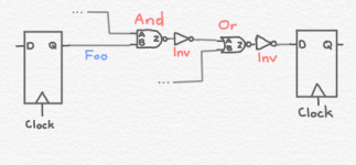
Above we have an example of a timing path isolated from a logic circuit. This path starts at a flip flop on the left. A flip flop is a logic circuit that holds a particular value until a clock signal transitions from one value to another. For example, if there is a logical 1 at the input, D, at the point of time when the clock input transitions from a 0 to a 1, then the flip flop will store a logical 1, which it will make available at its output, Q. If the input, D, changes value to a logical 0, this is ignored by the flip flop. The flip flop only cares about what happens when its clock transitions from a 0 to a 1. (Flip flops can be designed to respond to either type of clock transition, so it could be 1 to 0 instead).
Once the clock transitions from a 0 to 1, the CPU clock cycle starts, and the path has to produce its final value by the time the clock again transitions from a 0 to a 1. This is because the path ends at another flip flop. The value at the input, D, of this flip flop, has to be correct by the time the second flip flop receives a clock transition from 0 to 1.
The clock frequency is the inverse of the period of the clock, and the period of the clock is how much time you have to complete all of the logic calculations on a timing path. So if your clock is 1 GHz, you have 1000 picoseconds for your timing path.
Here’s what needs to be done in that time:
Note that the And gate and the Or gate have other inputs not discussed here. Those would be part of other, different timing paths, which may be more or less critical than the timing path we are looking at.
Right of the bat, a good logic designer sees potential issues with this logic path. The first thing I’ll ask is - what, exactly, is an And gate?
The table above is the truth table for a 2-input And gate. It shows the value of Z depending on the values of A and B. If my current value of Z is a 1, then it will switch to a 0 if either A or B switch to 0’s. And if my current value of Z is a 0, then it will switch to 1 if A or B switches to 1 (as long as the other of A or B is already a 1 or also switches to 1). In other words, the inputs and outputs switch in the same direction.
But CMOS doesn’t work that way. Below is the schematic for a 2-input CMOS And gate.

Schematic for a 2-input CMOS And gate
As shown in this schematic, this is always implemented as two different gates - a 2-input Nand gate followed by an inverter. The 2-input Nand gate produces the opposite values of a 2-input And gate. The inverter is required in order to flip the value of X - the output of the Nand - to the opposite value, to produce the required values for Z.
This takes extra delay. First the Nand has to produce its result, and then the inverter produces its result. The total delay is thus the Td for the Nand, plus the Td for the inverter.
The same thing holds true for the 2-input Or gate. This is really implemented as a 2-input Nor gate followed by an inverter.
Our timing path, therefore, is really as follows.

The advantage of combining the Nand with an Inv to create an And gate is that you might save a little space. The huge disadvantage is that, unless your And gate is very close to the gates that follow it in the path, you are not optimally driving the downstream logic. Consider the following situation:

Not a great solution for driving a long wire
Here we’ve created an And gate by shoving an inverter very close to a Nand gate. We then drive a long wire with the output of the inverter stage of the And gate. In order to drive the long wire, the inverter has to be very big - it needs to be able to move a lot of charge quickly in order to for the input to the ”Next Gate” to have a reasonably fast slope.
A better solution would be to move the inverter half way along the long wire, using it as a repeater. Because the effects of the long wire are not linear, this means that the circuit, overall, uses a lot less current.

A better solution for driving a long wire
But there are other considerations as well. Why are we using And and Or gates in the first place? Perhaps the architect's model contained an expression like:
Result := (Foo & X) | Y
That expression could have been written lots of other ways, but most people think in terms of positive logic - And, Or, etc.
A logic designer, however, has to be able to switch between positive and negative logic freely, for multiple reasons. Consider the Or gate that we've replaced with a Nor gate followed by an inverter. It turns out that Nor, which performs the function Not(A Or B), is logically equivalent to (not A and not B). We can use this fact to get rid of the inverters in our path, assuming we don't want to keep them to act as repeaters. The following sequence shows how this can be done:

Replace the Nor with an And, and invert both the And's inputs

Replace the And with a Nand followed by an inverter

Pairs of inverters cancel out
We've eliminate the inverters, corresponding to two gate delays, from this path, at the cost of adding an inverter to another path (the path that goes through the B input of the second Nand). It turns out that, for reasons too complicated to explain in Part 2 of this series, Nand gates are also preferable to Nor gates. The short answer is Nor gates will be bigger and more power-hungry. So we've benefited this particular path quite a bit, assuming we don't have to drive long wires that would have benefited from the inverter "repeaters."
it's also possible that the B-input to the second Nand gate was already available in inverted form, meaning we may not even have had to add an inverter to that other path.
The point of all this was not to provide a "best" solution to this particular toy design, but to give the reader a flavor of the kinds of things that logic designers must think about.
The following diagram illustrates how the parasitics associated with a wire can affect the timing behavior of the logic circuit.

In addition to the transition being delayed the further you go down the wire, the actual transition from high-to-low takes longer. This effect is very pronounced on long wires, and logic designers take care to compensate for this issue.
Additionally, much of the parasitic capacitance on the wire comes from capacitive coupling to neighboring wires. If the neighboring wires are correlated, so that they are all likely to switch at the same time, and mostly in one direction, this can inject noise onto a wire and greatly affect the behavior of the circuit. A very wise man once proved that the effective capacitance seen by a wire can be triple the actual capacitance, depending on how fast the edge rates are on the “victim” wire and the “aggressor” wires. “A 533-MHz BiCMOS Superscalar RISC Microprocessor,” C. Maier et al., IEEE Journal of Solid State Physics, Nov. 1997, p. 1631.
Additionally, this noise can actually break the functionality of the circuit (a problem that actually occurred in the second tape-out of the Exponential x704 processor). The neighboring wires can inject a noise pulse onto the victim wire that, if it occurs at the wrong time, causes a wire to incorrectly look like a 1 or a 0.
The logic designer is responsible for producing an actual design that behaves in the way the architects intended. This involves designing logic circuits, figuring out how to physically implement the logic circuits, and making sure the circuits meet various constraints (including timing, power, area, and other electrical issues).
Types of Blocks on a CPU
CPU physical/logical design work can be roughly divided into two types of methodologies that correspond to two different types of blocks: standard cell blocks and macros. Macros are typically things like RAMs, clock generation circuitry, and other blocks where the design is done on a transistor-by-transistor basis, a polygon at a time, often because analog effects dominate over digital effects, and a higher-level approach would be problematic. For example, the design work I did at Sun on a Sparc microprocessor involved the transistor-level design of a content-addressable memory for use in the reservation stations. This type of work is usually performed by circuit designers, often at the direction of logic designers who provide guidance as to functionality and constraints.The standard-cell blocks are created by arraying a set of “standard cells,” each of which corresponds to one or more logic gates, much like one builds a house out of Lego bricks. The individual cells usually correspond to simple logic functions, seldom with more than 5 or 6 inputs and 1 or 2 outputs, and most standard cells have just two or three inputs and one output. Standard cells usually have names like NAND2x1, NAND2x2, and INVx4. The logic function is indicated by the start of the name, the number of inputs comes before the “x,” and the number after the “x” is the strength of the gate (corresponding to the relative size of its transistors).
Example standard cell dimensions from a TSMC standard cell library
Typically, each standard cell has the same height, so that they can be arrayed in rows, but the width of standard cells may vary. A power rail and a ground rail are found at the top and bottom of each cell, so that when the cells abit a complete horizontal power rail and ground rail is formed.
At the companies I worked at, we designed the standard cells ourselves. This involved creating circuit diagrams for each cell, laying out the cell (i.e. generating the necessary polygons on each layer), and characterizing the electrical behavior of each cell. Companies may also use standard cell libraries provided by whatever fab they are using.
The process used to generate standard cell-based designs is iterative. The following loop is performed until all timing and electrical requirements are achieved.
- Generate a “netlist,” which indicates each cell to be used, its strength, and to what other cells it is connected. This process is sometimes called “synthesis.” We always did it by hand (using algorithms like The Quine-McCluskey algorithm, and a general knowledge and understanding of Boolean math). Many companies use automated tools such as those sold by Synopsys.
- ”Place” the cells. In other words, arrange them in a stack of rows that fills the allotted floor plan area for the block.
- ”Route” the block. This involves creating wires in various metal layers so that each of the netlist connections is achieved.
- Perform parasitics extraction. This models each wire as a distributed resistor-capacitor network based on the parasitic resistances and capacitances of the wires.
- Perform static timing analysis. This looks at every logic path and figures out how much time each takes.
- Perform other analyses. For example, electromigration, power-rail voltage droop, design rule checking, layout-vs-schematic checking, formal verification, etc.
Constraints
The logic designer is responsible for designing parts of the chip subject to various constraints. Because there are so many constraints that need to be satisfied, and because there are so many degrees of design freedom, logic design can be very difficult, and tools that claim to completely automate the process invariably do a worse job than well-trained engineers.Floor plan for the Exponential x704
These constraints include:
- The area (and shape of the area) allotted for the logic. This is reflected in the overall floor plan.
- The need for the logic to perform its function within the allotted clock cycle
- Power consumption limitations
- Thermal limitations
- Reliability concerns, such as minimizing electromigration and hot carrier effects
- Power supply limitations, including minimizing “IR drop”
- A limited number of metal layers with which to build the necessary circuit interconnections
- Correct functionality. The logic has to be right, and has to work properly regardless of external influences (radiation, temperature fluctuations, electrical noise, power supply variations).
- The semiconductor process being used. There are numerous “design rules” that determine how the circuit can be physically formed, and determine how it electrically operates.
- Manufacturability. In order to obtain good fab yields, there are limitations on how one can design circuits, and various rules that must be met in order to ensure that a sufficient quantity of die on each wafer work properly.
Design Considerations
Below I’ll walk through some of the factors that a high-end CPU designer considers when performing design work.
Cell Delays

Consider an inverter, the simplest CMOS logic gate. An inverter simply produces, as its output, the opposite logic value of its input. A rising voltage on the input of an inverter, for example, produces a falling output on the output of the inverter. In the above figure, the inverter has input A and output Z. The top graph shows a rising edge on the input of the inverter. As shown in the bottom graph, this produces a falling edge on the output of the inverter.From the perspective of a logic designer, there are multiple considerations here. We need to understand the timing relationship between the waveform on the input and the waveform on the output. The way this is typically modelled is by defining two relevant timing characteristics. The first is the delay from the input to the output, indicated above as Td. This is usually measured by finding the point in time at which the input waveform has reached the midpoint between the ground voltage and the power supply voltage, finding the point in time at which the output waveform reaches the same voltage, and measuring how much time elapsed between those two events.
Td will vary depending on multiple factors, including how fast the input voltage rises and how much capacitive load is found on the output of the logic gate (e.g. from connecting to inputs of other gates and driving metal wires).
To enable design tools to accurately model the timing behavior of a proposed design, when the logic cells are designed they are characterized by, among other things, performing a series of experiments, varying the input waveform and output capacitive loading, to measure Td (using a tool called SPICE), and creating tables that can be consulted to figure out what Td should be given the particular manner in which a logic gate is used.
The second relevant measurement is shown on the above graph as Ts. This is sometimes called the edge rate, slew rate, or rise/fall time of the gate. This is a measure of how long it takes the output to complete its transitIon. Typically this measurement is started when the waveform reaches 10% or 20% of its transition, and is stopped when the waveform reaches 80% or 90% of its intended transition. This value is important because the longer it takes the output to transition, the longer it will take subsequent gates which receive this waveform on their inputs to transition. As with Td, different values of Ts are calculated during characterization of the logic gates, and stored in tables.
Timing Paths
Logic gates cannot be considered in isolation. Each is part of one or more “paths” between clocked state elements. Each logic gate affects the behavior of the gates that come before it in the path (by adding capacitive load to the prior gates) and the behavior of the gates that come after it in the path (by determining the waveform at the inputs of those gates).An optimal design makes each gate as big as it has to be in order for the timing goals to be met, but no bigger than it has to be - if gates are too big, then power consumption and heat increases, and secondary effects such as voltage droop on the power rails can become a problem.
Simply increasing the power of a logic gate often will speed up the path, but it may slow it down instead, by slowing down the gates that come before it In the logic path.
Above we have an example of a timing path isolated from a logic circuit. This path starts at a flip flop on the left. A flip flop is a logic circuit that holds a particular value until a clock signal transitions from one value to another. For example, if there is a logical 1 at the input, D, at the point of time when the clock input transitions from a 0 to a 1, then the flip flop will store a logical 1, which it will make available at its output, Q. If the input, D, changes value to a logical 0, this is ignored by the flip flop. The flip flop only cares about what happens when its clock transitions from a 0 to a 1. (Flip flops can be designed to respond to either type of clock transition, so it could be 1 to 0 instead).
Once the clock transitions from a 0 to 1, the CPU clock cycle starts, and the path has to produce its final value by the time the clock again transitions from a 0 to a 1. This is because the path ends at another flip flop. The value at the input, D, of this flip flop, has to be correct by the time the second flip flop receives a clock transition from 0 to 1.
The clock frequency is the inverse of the period of the clock, and the period of the clock is how much time you have to complete all of the logic calculations on a timing path. So if your clock is 1 GHz, you have 1000 picoseconds for your timing path.
Here’s what needs to be done in that time:
| Starting Flip Flop Setup Time - the time it takes from the clock transition until Q is stable |
| Flip Flop Q—>Input B of the And gate (the time it takes the signal to travel on the wire Foo) |
| And gate B—>Z (the Td for the And gate) |
| And gate Z—>Input A of the Or gate (the time it takes the signal to travel on the wire Bar) |
| Or gate A—>Z (the Td for the Or gate) |
| Or gate Z—>Flip flop D (the time it takes the signal to travel on the wire Result) |
| Hold time of the second flip flop - the amount of time the input must be stable on the D input prior to the clock transition, in order for the flip flop to correctly grab it |
Note that the And gate and the Or gate have other inputs not discussed here. Those would be part of other, different timing paths, which may be more or less critical than the timing path we are looking at.
Right of the bat, a good logic designer sees potential issues with this logic path. The first thing I’ll ask is - what, exactly, is an And gate?
CMOS logic gates are always inverting. That means a rising input edge cannot cause a rising output edge. It is impossible to implement a CMOS And gate because the boolean AND function is non-inverting:A | B | Z |
|---|---|---|
0 | 0 | 0 |
0 | 1 | 0 |
1 | 0 | 0 |
1 | 1 | 1 |
The table above is the truth table for a 2-input And gate. It shows the value of Z depending on the values of A and B. If my current value of Z is a 1, then it will switch to a 0 if either A or B switch to 0’s. And if my current value of Z is a 0, then it will switch to 1 if A or B switches to 1 (as long as the other of A or B is already a 1 or also switches to 1). In other words, the inputs and outputs switch in the same direction.
But CMOS doesn’t work that way. Below is the schematic for a 2-input CMOS And gate.
Schematic for a 2-input CMOS And gate
As shown in this schematic, this is always implemented as two different gates - a 2-input Nand gate followed by an inverter. The 2-input Nand gate produces the opposite values of a 2-input And gate. The inverter is required in order to flip the value of X - the output of the Nand - to the opposite value, to produce the required values for Z.
This takes extra delay. First the Nand has to produce its result, and then the inverter produces its result. The total delay is thus the Td for the Nand, plus the Td for the inverter.
The same thing holds true for the 2-input Or gate. This is really implemented as a 2-input Nor gate followed by an inverter.
Our timing path, therefore, is really as follows.
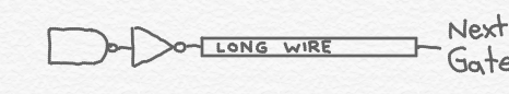
The advantage of combining the Nand with an Inv to create an And gate is that you might save a little space. The huge disadvantage is that, unless your And gate is very close to the gates that follow it in the path, you are not optimally driving the downstream logic. Consider the following situation:
Not a great solution for driving a long wire
Here we’ve created an And gate by shoving an inverter very close to a Nand gate. We then drive a long wire with the output of the inverter stage of the And gate. In order to drive the long wire, the inverter has to be very big - it needs to be able to move a lot of charge quickly in order to for the input to the ”Next Gate” to have a reasonably fast slope.
A better solution would be to move the inverter half way along the long wire, using it as a repeater. Because the effects of the long wire are not linear, this means that the circuit, overall, uses a lot less current.
A better solution for driving a long wire
Result := (Foo & X) | Y
That expression could have been written lots of other ways, but most people think in terms of positive logic - And, Or, etc.
A logic designer, however, has to be able to switch between positive and negative logic freely, for multiple reasons. Consider the Or gate that we've replaced with a Nor gate followed by an inverter. It turns out that Nor, which performs the function Not(A Or B), is logically equivalent to (not A and not B). We can use this fact to get rid of the inverters in our path, assuming we don't want to keep them to act as repeaters. The following sequence shows how this can be done:
Replace the Nor with an And, and invert both the And's inputs
Replace the And with a Nand followed by an inverter
Pairs of inverters cancel out
We've eliminate the inverters, corresponding to two gate delays, from this path, at the cost of adding an inverter to another path (the path that goes through the B input of the second Nand). It turns out that, for reasons too complicated to explain in Part 2 of this series, Nand gates are also preferable to Nor gates. The short answer is Nor gates will be bigger and more power-hungry. So we've benefited this particular path quite a bit, assuming we don't have to drive long wires that would have benefited from the inverter "repeaters."
it's also possible that the B-input to the second Nand gate was already available in inverted form, meaning we may not even have had to add an inverter to that other path.
The point of all this was not to provide a "best" solution to this particular toy design, but to give the reader a flavor of the kinds of things that logic designers must think about.
Wires
The next article in this series will get into much more detail on the physical design flow, but as discussed above, wires are an important consideration in logic design. The waveforms on the outputs of logic gates are quite different when taking wires into account. The issue is that all of the wires that are used to connect the gates have parasitic impedences that affect the electrical behavior of the circuit. These are typically modeled as a series of resistors and capacitors (an “RC network“) using a parasitics extraction tool that analyzes the wires, and then the RC network is typically fed into a static timing tool like Synopsys’ Primetime tool or the in-house tools I wrote at AMD (“Mr. Bigglesworth” and “Wanda”) to predict the timing behavior of the circuit.The following diagram illustrates how the parasitics associated with a wire can affect the timing behavior of the logic circuit.
In addition to the transition being delayed the further you go down the wire, the actual transition from high-to-low takes longer. This effect is very pronounced on long wires, and logic designers take care to compensate for this issue.
Additionally, much of the parasitic capacitance on the wire comes from capacitive coupling to neighboring wires. If the neighboring wires are correlated, so that they are all likely to switch at the same time, and mostly in one direction, this can inject noise onto a wire and greatly affect the behavior of the circuit. A very wise man once proved that the effective capacitance seen by a wire can be triple the actual capacitance, depending on how fast the edge rates are on the “victim” wire and the “aggressor” wires. “A 533-MHz BiCMOS Superscalar RISC Microprocessor,” C. Maier et al., IEEE Journal of Solid State Physics, Nov. 1997, p. 1631.
Additionally, this noise can actually break the functionality of the circuit (a problem that actually occurred in the second tape-out of the Exponential x704 processor). The neighboring wires can inject a noise pulse onto the victim wire that, if it occurs at the wrong time, causes a wire to incorrectly look like a 1 or a 0.