Apple M5 rumors

dada_dave

Elite Member
Joined
Oct 25, 2022
Posts
3,268
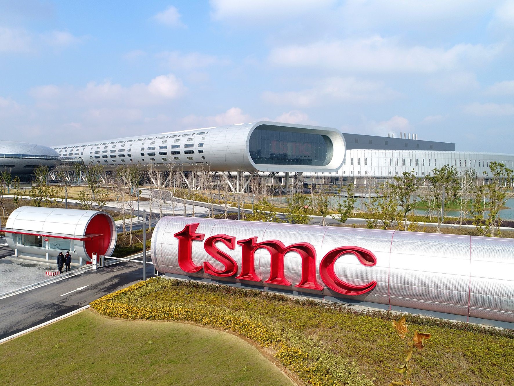
Here’s one (or two really) to start off with. Strictly speaking this particular rumor is more about TSMC, but it encompasses Apple products which I think was the most interesting/surprising part if a little discordant with the other mentioned M5 rumor:

Apple​

Unsurprisingly, Apple will be one of the first companies to adopt TSMC's N2 node. It will tape out in December 2024 and be used for the Apple A20 Pro and Apple M5. The former will enter mass production in late 2025, while the latter will have to wait until Q2, 2026. This sits in line with an earlier report which said Apple M5-powered iPads are scheduled to launch in late 2025. Additionally, it also debunks another one talking about Apple using an Intel node for the A20 Pro, which will power 2026's iPhone 18 series.

It would appear to me that M5-based iPads launching in late 2025 would not be in fact consistent with Q2 2026 M5 manufacturing. Given the proposed timeline, N2 would seem to be a better fit for M6 than M5 unless Apple is going to skip N3P and the A19 core architecture for M5. That is possible. Again though M5 based iPads in late 2025 would not fit that rumor. I would also say that given the presence of seemingly M5-based Mac-IDs in the macOS firmware, it would be unlikely that Apple will be waiting until 2026 to launch M5s.

Of more tangential note to this topic is that according to this rumor Intel is still slated to use TSMC 2nm while Qualcomm is not.
 
Last edited:
N2 will by all reports be ready to go for next year. And both N2P and A16 are on track for 2026. So going with N3P in 2025 and then N2 in 2026 puts them a year behind the cutting edge for two consecutive years.

A16 is the node with the biggest wildcard with backside power delivery. So it would make sense to me to do:
M5 = N2
M6 = N2P
M7 = A16 (after all the kinks are worked out).

I wonder when in 2025 they’ll have the kinks worked out. In any event, whatever the decision is for M5, Apple made it a long time ago.
 
N2 will by all reports be ready to go for next year. And both N2P and A16 are on track for 2026. So going with N3P in 2025 and then N2 in 2026 puts them a year behind the cutting edge for two consecutive years.

A16 is the node with the biggest wildcard with backside power delivery. So it would make sense to me to do:
M5 = N2
M6 = N2P
M7 = A16 (after all the kinks are worked out).
Welcome to the forums!

N2 starts tape out at the end of this year, which is initial low volume production only for testing chips and the node. Mass production of N2 though won’t be available until the end of next year for production of 2026 devices. Thus the earliest time frame we could reasonably expect N2 devices would be spring of 2026 similar to how the iPad Pro launched M4 in Spring of 2024 with N3E which was available for mass production at the end of 2023. Under that scenario it is possible that M5 will be similar to M3 and M6 would launch in 2026. It is also possible that M-chips will skip the 2025 core-node but that doesn’t fit the other rumors or known facts.

N2P and A16 will supposedly be available simultaneously but may be targeting different markets initially. As you say, the kinks for A16 are more substantial but TSMC has assured its customers and investors it will be available for a certain class of chips at the same time (larger data center chips). So indeed that may not include Apple chips until later but if so then that would push Apple’s use of A16 back to 2028 and M8.

Prospective calendar:

End of 2024 - N3P available

2025 - M5/A19 based on N3P, N2 available at end of 2025

2026 - M6/A20 based on N2, A16/N2P available at end of 2026

2027 - M7/A21 based on N2P or maybe A16

2028 - M8/A22 based on A16 or follow on node
 
So which of these nodes will Apple use for a chiplet-based desktop/workstation build, gotta pump up the GPU core count...
 
Mass production of N2 though won’t be available until the end of next year for production of 2026 devices.
My understanding was that volume production would start towards the beginning of H2 - too late for A series chips that debut in early September, but just right for the early November timeline that Apple has used for the last couple M series reveals.

I think it boils down to whether Apple sees value in leading with the M series instead of the A series. The M4 showed that there’s very little if any Osborne effect on the iPhone as a result of M series CPU core designs appearing ahead of the A series debut.

So the question becomes “do they want to be aggressive or not”? My backyard quarterbacking says “aggressive on N2 and N2P, risk averse on A16.”

From what I’ve seen N2 will be “late 2025”. Which has been TSMC’s typical pattern the last few nodes. Regardless it would be highly unusual for Apple to split the A-series and M-series by node with launches so close together. It’s not impossible, but it doesn’t seem likely especially not on top of the tight timeframe.

It’d be fun though to have either the same core design on two different nodes or two core designs back to back, even closer than the M3 and M4. I just don’t see it as the most likely outcome.
 
A pair of Macrumors articles on M5:


The second dual-use article for M5 is interesting ... though its support for the M5 in particular having dual use design is lacking (no link for Economics Daily and the Digitimes article is paywalled and the links that do work say that M4 will also be dual use so that's not necessarily a feature of M5 vs M4).

Also odd is the insistence that Apple is not using N2 "for cost reasons". I don't see any support for that either, but it could be in a paywalled link. No one else is rumored to release products on N2 that early or even in early 2026. Given Apple's penchant for using TSMC's latest and greatest (and paying a lot for the privilege to be first), it's more likely that the node simply isn't ready for high volume manufacturing for a late 2025 product.

Kuo doesn't explicitly state that the iPad Pro is coming out in 2H25, but that's a reasonable interpretation of what he said:

3. The iPad Pro equipped with the M5 processor is expected to enter mass production in 2H25. The company’s business momentum in 2H25 is anticipated to benefit significantly from Apple’s new product launches.

And fits with earlier rumors of a late 2025 M5 iPad Pro.
 
If this happens to the M-series chips it will be after M5 (the article claims it will appear in the iPhone in 2026), but since this thread is more generally about future chip design, I'm posting it here.

It says Apple is working with Samsung to move RAM off the SoC to increase the number of pins and thus the bandwidth. But I thought Apple's UMA required memory to be positioned close to the chip to minimize latency, and this change would increase the distance between processor and RAM:

"PoP is not optimal for on-device AI. Bandwidth is determined by data transfer speed, data bus width, and data transmission channels. Bus width and channel are determined by the number of I/O pins. To increase the number of pins, the package needs to become larger. But in PoP, the memory’s size is determined by the SoC, which limits the number of I/O pins on the package...

Discrete package also provides better heat regulation. On-device AI’s parallel processing causes high levels of heat. Having a larger surface for the memory allows heat to emitted in a wider surface.

However, there are downsides, which is that the distance between the memory and SoC becomes longer. Mac and iPads used discrete package but then changed it to memory-on-package (MOP) with M1 SoC. Using MOP, which shortens the distance between the chips, reduces latency, and minimizes power loss."

Thoughts?

 
Last edited:
If this happens to the M-series chips it will be after M5 (the article claims it will appear in the iPhone in 2026), but since this thread is more generally about future chip design, I'm posting it here.

It says Apple is working with Samsung to move RAM off the SoC to increase the number of pins and thus the bandwidth. But I thought Apple's UMA required memory to be positioned close to the chip to minimize latency, and this change would increase the distance between processor and RAM:

"PoP is not optimal for on-device AI. Bandwidth is determined by data transfer speed, data bus width, and data transmission channels. Bus width and channel are determined by the number of I/O pins. To increase the number of pins, the package needs to become larger. But in PoP, the memory’s size is determined by the SoC, which limits the number of I/O pins on the package...

Discrete package also provides better heat regulation. On-device AI’s parallel processing causes high levels of heat. Having a larger surface for the memory allows heat to emitted in a wider surface.

However, there are downsides, which is that the distance between the memory and SoC becomes longer. Mac and iPads used discrete package but then changed it to memory-on-package (MOP) with M1 SoC. Using MOP, which shortens the distance between the chips, reduces latency, and minimizes power loss."

Thoughts?


i saw this. and i know a lot about apple’s packaging. I think the explanation given is a little confusing and misleading. The issue is that the memory chips are in their own little packages, which are then inside the SoC package. So to add I/O to the memory chips, the memory chip sub-packages would have to get bigger. This would then require the SoC package to get bigger. On a system level, I guess, Apple may find it preferable to not do that; but taking the RAM out of the package means that the combined RAM+SoC take more volume than if they were in the same SoC package (even if you had to expand the size of the SoC package to make it work). Which makes me think something is off about this rumor.

What would be a far better solution than moving the memory out of the package would be to remove it from its little subpackage, and then you can have as many I/Os as you want on the RAM chips without growing the size of the SoC package.

As for latency, it’s 6 picoseconds or so for each millimeter of additional distance, so if the RAM is still close to the CPU, it wouldn’t make a tremendous difference in timing; and since performance = f(bandwidth/latency), and this scheme could, for example, double bandwidth while increasing latency by only a few percent, that part doesn’t trouble me.
 
Moving RAM off-package could be a step toward adopting a matured NVM architecture such as SOT or STT MRAM. These types are currently about DDR4 speeds and could maybe become viable as a Flash replacement in the next few years while also providing useful RAM space, but the system design would have to change quite a lot to make it work well. If it can manage to take hold, it will be a game changer, and Apple will want to be out front.
 
i saw this. and i know a lot about apple’s packaging. I think the explanation given is a little confusing and misleading. The issue is that the memory chips are in their own little packages, which are then inside the SoC package. So to add I/O to the memory chips, the memory chip sub-packages would have to get bigger. This would then require the SoC package to get bigger. On a system level, I guess, Apple may find it preferable to not do that; but taking the RAM out of the package means that the combined RAM+SoC take more volume than if they were in the same SoC package (even if you had to expand the size of the SoC package to make it work). Which makes me think something is off about this rumor.

What would be a far better solution than moving the memory out of the package would be to remove it from its little subpackage, and then you can have as many I/Os as you want on the RAM chips without growing the size of the SoC package.

As for latency, it’s 6 picoseconds or so for each millimeter of additional distance, so if the RAM is still close to the CPU, it wouldn’t make a tremendous difference in timing; and since performance = f(bandwidth/latency), and this scheme could, for example, double bandwidth while increasing latency by only a few percent, that part doesn’t trouble me.
So if they keep the RAM in the subpackages, they'd need to make the subpackages bigger to add I/O; but there's no reason they couldn't do that while keeping it on the SoC (just requires making the SoC bigger); and, additionally, the net result would be less total volume than if they moved it off-package. Yeah, I was wondering about that as well--if they want to keep the RAM in the subpackages but add I/O, why not just make the SoC larger?

But if they remove the RAM from the subpackages, then they can add I/O while keeping the RAM volume the same, i.e., the RAM volume becomes I/O-independent. If so, why use the subpackages in the first place? Is it because, with the current number of pins, the RAM volume is smaller when it's kept inside the subpackages, and that this volume advantage is only lost with a high number of pins?
 
Last edited:
So if they keep the RAM in the subpackages, they'd need to make the subpackages bigger to add I/O; but there's no reason they couldn't do that while keeping it on the SoC (just requires making the SoC bigger); and, additionally, the net result would be less total volume than if they moved it off-package. Yeah, I was wondering about that as well--if they want to keep the RAM in the subpackages but add I/O, why not just make the SoC larger?

But if they remove the RAM from the subpackages, then they can add I/O while keeping the RAM volume the same, i.e., the RAM volume becomes I/O-independent. If so, why use the subpackages in the first place? Is it because, with the current number of pins, the RAM volume is smaller when it's kept inside the subpackages, and that this volume advantage is only lost with a high number of pins?
I think the reason they keep the RAM in the subpackages is because that’s what’s for sale. They don’t buy full-custom RAM chips, with contact locations where they want them, etc. Maybe someday they’ll get into custom RAM chips.

Anyway, if this rumor is true, I’d love a clearer explanation of what’s going on. The one provided so far doesn’t make too much sense to me.
They sort of did with the R1 right?

@Jimmyjames’ thread

 
They sort of did with the R1 right?

@Jimmyjames’ thread

yeah, i forgot about R1.
 
I can't read the article on thelec.com. It says it's not available. I've seen the articles on MR and AI. They read like gibberish, because the authors are too ignorant. As several people here have said, what we're seeing so far makes no sense.

I'm not convinced there's anything behind these rumors at all, but if there are, my guess is that it's an issue of heat management in concert with energy use, with any bandwidth improvement a secondary issue. (Take the heat off the SoC, but then pay a price in energy with the longer path. Go slow/wide to counter that and get somewhat more BW at the same time. Pay with a bit of latency.)

The most interesting part of this for me is the brief mention of PIM. It's hard to see a path to horizontal market viability for PIM, but if anyone can do it, it's Apple. And the performance advantages are potentially enormous.

There's also the possibility that we wind up using CAMMs. If so, 50-50 Apple uses their own pinout to force incompatibility.
 
I can't read the article on thelec.com. It says it's not available. I've seen the articles on MR and AI. They read like gibberish, because the authors are too ignorant. As several people here have said, what we're seeing so far makes no sense.

I thought it was particularly frustrating since it shows that most people don't pay any attention at all. Already the article made little sense, MR just copied it blindly , and the MR forum crowd interpreted it in the most ridiculous ways possible. I am very glad that there are smaller communities like this one, where people actually think and try to understand what things mean.
 
I thought it was particularly frustrating since it shows that most people don't pay any attention at all. Already the article made little sense, MR just copied it blindly , and the MR forum crowd interpreted it in the most ridiculous ways possible. I am very glad that there are smaller communities like this one, where people actually think and try to understand what things mean.
the given explanation is also a little silly when one considers that you have to connect to these new external rams somehow, which means you have to put a ton of new contacts on the exterior of your SoC package. These take up just as much room as the contacts would have taken on the (internal) RAM subpackages, if not more (because their size would likely be bigger to accommodate thicker wire traces). So you may have to grow the size of your SoC package to accommodate this, in any case.
 
Looks like TSMC 2nm yields are pretty good at this point. Supposedly 60%. I’ve fabbed many cpus on 60%-yielding processes. But I’m sure they’ll get to 80% within 6 months if this is true.

 
Back
Top