Apple M5 rumors

This is from an Apple patent and closely matches what you would see in A-series packages of late:

Screenshot 2024-12-06 at 8.08.11 AM.png


If you look at item 155, that’s a contact to the SoC (150). You can see how much smaller that is than the contacts to the package (190). The RAM would be, for example, 110.
 
From what I have seen of die shots, the memory controllers are proximal to the GPU cores, which are near the top level cache; all the device controllers (TB, E-Net, USB, etc) are at the other end of the chip. Which makes sense. What the advantage (for Apple, and for performance) in having RAM in POP or CAMM is not clear.
 
Well, it's obvious why the SLC is near the memory controllers. Placement of the GPU may be coincidental, or it may be that GPUs being the biggest consumers of memory bandwidth, at least in some scenarios, makes that actually worthwhile.

I suspect there is a modest but measurable advantage to having the RAM mounted PoP, as opposed to using CAMMs - the shorter distance probably allows for a lower pJ/b. I don't know that for sure though. (@Cmaier?) Whether that's enough to matter is another thing entirely.

I really think this entire story is garbled nonsense. We already have Mx chips with 512-bit-wide memory, successfully delivering devastating bandwidth numbers. Apple knows how to do this, and they are doing it already. And guess what? They're not using vias, it's all shoreline. So chip area is not a major factor, though chip perimeter might be. They could at least in part solve that by making chips much less square, giving each one more perimeter for the same area.

Now, is this substantially different from what they're doing with Ax chips? It does seem so, and maybe with them area really is a limiting factor. But it's not like they don't already know how to do it another way. So if bandwidth really does motivate them, then... it still plays out like I said in my last post.
 
From what I have seen of die shots, the memory controllers are proximal to the GPU cores, which are near the top level cache; all the device controllers (TB, E-Net, USB, etc) are at the other end of the chip. Which makes sense. What the advantage (for Apple, and for performance) in having RAM in POP or CAMM is not clear.

Memory controllers and SLC are tightly coupled: controllers essentially “own” a portion of SLC. All hardware addresses associated with a specific controller can only be cached in its SLC block. Keeping them close can save a good chunk of wiring I suppose.
 
Well, it's obvious why the SLC is near the memory controllers. Placement of the GPU may be coincidental, or it may be that GPUs being the biggest consumers of memory bandwidth, at least in some scenarios, makes that actually worthwhile.

I suspect there is a modest but measurable advantage to having the RAM mounted PoP, as opposed to using CAMMs - the shorter distance probably allows for a lower pJ/b. I don't know that for sure though. (@Cmaier?) Whether that's enough to matter is another thing entirely.

I really think this entire story is garbled nonsense. We already have Mx chips with 512-bit-wide memory, successfully delivering devastating bandwidth numbers. Apple knows how to do this, and they are doing it already. And guess what? They're not using vias, it's all shoreline. So chip area is not a major factor, though chip perimeter might be. They could at least in part solve that by making chips much less square, giving each one more perimeter for the same area.

Now, is this substantially different from what they're doing with Ax chips? It does seem so, and maybe with them area really is a limiting factor. But it's not like they don't already know how to do it another way. So if bandwidth really does motivate them, then... it still plays out like I said in my last post.
Yes, big power bump needed if you move the ram out. Look at the size of those package contacts. Wires that connect to them are also big. Lots of parasitic capacitance you need to drive. Whether that’s a huge deal when your system power consists of many contributions- who knows.

As for chip aspect ratio, remember that the reticle is squarish. Not a big concern for A-series of course. But aa you note, they could move to packaging more similar to M-series and that would still make more sense than what is being described here (maybe. I’m not sure what goes into finding volume to shove all the components into a thin phone)
 
Is that necessary? Can't you make non-squarish rectangular chips as long as you're not running up against either of the maximum reticle dimensions?
Yeah, like i said, it’s not really too much of an issue for the A-series chips, and more a worry for things like the bigger versions of the M-series chips.

Still, though, you pay per wafer start, so you want as many die on the wafer as possible. So, you don’t want something like this - it’s potentially easier to fill the space with squares:

1733595658977.png
 
What is the cost of a heterogenous wafer? By which I mean, if you set it up to burn a CPU block and a distinct GPU block (different masks) and an interconnect on the wafer, could they leapfrog the reticle limit without too high ap performance/production cost?
 
Is that necessary? Can't you make non-squarish rectangular chips as long as you're not running up against either of the maximum reticle dimensions?
That raises an interesting question. In a rectangle, the average pairwise distance (i.e., the average straightline distance between any two points on the surface) is minimized if it's a square. The seems beneficial for intrachip communicatiion.

So what design considerations would motivate a non-square design? The most obvious one would be that, for a given area, the less square it is, the bigger the perimeter, and thus the more room for I/O. Are there any modern chip designs that aren't square and, if so, what would be the reason for this?

Also, anyone know if the tiling is worse if the chip isn't square (fewer chips/wafer)?
 
Last edited:
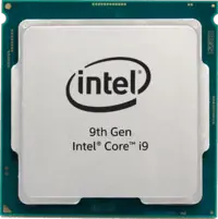
Intel spent quite a long time being fond of highly non-square layouts in client CPUs. Here's a typical example: the i9-9900K and similar Coffee Lake family members (scroll down for the die photo and an annotated version).


In the annotated version, the communcations structure is the small blocks labeled 'Ring Interconnect Agents'. Intel was, at the time, very fond of ring busses for on-die communications. Links are point-to-point between ring agents; packets are forwarded from agent to agent until they reach their destination.

Intel managed to do a reasonable job of minimizing the total length of this ring interconnect by laying it out as the 'spine' of this chip, keeping it all very central. I'm not sure there would be an advantage to a more square relayout of the same blocks; in fact I suspect it would force some ring bus links to be quite a bit longer.

re: tiling, it's not immediately obvious to me how much squareness matters. Empirically, skinny rectangles similar to the 9900K were the norm across many generations of Intel's high volume client segment products. That's exactly the market segment where Intel would be at its most cost conscious, so I'm willing to handwave that if there's a tiling penalty, it's either small or can be made small by careful tweaks to the rectangle's dimensions.

intel has a little bit of an advantage here re: tiling. They control the fab, so they can screw around with the reticle aspect ratio and dimensions if they need to.
 
What is the cost of a heterogenous wafer? By which I mean, if you set it up to burn a CPU block and a distinct GPU block (different masks) and an interconnect on the wafer, could they leapfrog the reticle limit without too high ap performance/production cost?
It's not only possible, it has been done. Cerebras is an AI-focused startup that worked in collaboration with TSMC to develop wafer-scale products.

It's not quite what you're talking about - it's homogeneous, not heterogeneous. They design one compute tile that's less than the reticle limit, and the wafer is full of copies of only that tile, nothing else. Communications between tiles use wires that pass through what would ordinarily be scribe lines.

TSMC also likes to run a prototyping service which runs a single wafer filled with chip designs from many different TSMC customers. It's almost certainly a lot more expensive per wafer, but by sharing one wafer across many prototypes, each client enjoys far lower cost to get some engineering samples. So long as each client doesn't need an entire wafer's worth of engineering samples, everyone wins.

For high volume manufacturing, though, the norm is one uniform device tiled across the whole wafer.
We used to fill little nooks with test structures. Helped us gauge manufacturing issues based on location on the wafer.
 
I’m curious, at wafer scale why don’t fabs fly test in an early metal layer and chemically mask good regions, then etch out bad regions for a redo? Alternatively, how do wafer scale fabs mitigate defects?
 
Last edited:
Still, though, you pay per wafer start, so you want as many die on the wafer as possible. So, you don’t want something like this - it’s potentially easier to fill the space with squares:
AFAIK, that's not generally true, though it's true more often than not. Tiling efficiency will vary for different rectangles (including squares as an instance of "rectangle"), given a particular diameter circle and required rectangle area. Squares may have a stronger advantage if you have to place all rectangles on a single grid (as opposed to different rows starting at different offsets) - which, come to think of it, may be true for all the wafers I've ever seen. Is that a necessity, the way they're manufactured?
 
AFAIK, that's not generally true, though it's true more often than not. Tiling efficiency will vary for different rectangles (including squares as an instance of "rectangle"), given a particular diameter circle and required rectangle area. Squares may have a stronger advantage if you have to place all rectangles on a single grid (as opposed to different rows starting at different offsets) - which, come to think of it, may be true for all the wafers I've ever seen. Is that a necessity, the way they're manufactured?
Not sure I understand your question entirely. The reticle repeats, and you can’t span two reticles, if that’s what you are asking (i,e, there’s a grid inherent from the fact that you are using a reticle). One other thing to keep in mind is you can’t rotate. (Well, you can, but there are very good reasons not to do that).
 
I’m curious, at wafer scale why don’t fabs fly test in an early metal layer and chemically mask good regions, then etch out bad regions for a redo? Alternatively, how do wafer scale fabs mitigate defects?
that would be outrageously expensive. And etching out a mistake would likely cause more problems to underlying layers.

typically all you can do is detective major screwups - a particular layer was too thin or thick - and then you discard the wafer.

also difficult to find defects during processing. you’d need an electron microscope if you are doing it visually. they are very very tiny, and the wafers are very big. And you can’t easily tell if a defect - say a screw dislocation - will affect anything.
 
I’m curious, at wafer scale why don’t fabs fly test in an early metal layer and chemically mask good regions, then etch out bad regions for a redo? Alternatively, how do wafer scale fabs mitigate defects?
Assuming the latter is referring to the Cerebras products I mentioned - I think they just build in lots of redundancy-based repairability, same as anyone else.

SRAMs are where you'll see it the most, and are an easy way to explain. Say your logic designer wants to put in a 1MiB SRAM array. The actual SRAM built by the memory compiler (or by hand, if you need more performance) can, on request, have extra capacity for redundancy. This is based on dividing it into smaller subarrays (in our 1MiB example, 64KiB would give us 16 smaller memories), adding one or two extra subarrays, and putting in the logic required to assemble any set of 16 subarrays into the final 1MiB memory. That logic is typically configured by some form of one-time programmable memory that gets written after testing the subarrays for functionality.
 
Not sure I understand your question entirely. The reticle repeats, and you can’t span two reticles, if that’s what you are asking (i,e, there’s a grid inherent from the fact that you are using a reticle). One other thing to keep in mind is you can’t rotate. (Well, you can, but there are very good reasons not to do that).
That's not what I was asking. Hm, let me try it this way.

Imagine that your grid of squares (just to keep this simple, but the same question goes for rectangles) is laid out over a circle. At row N (this is past the halfway point), you can fit exactly 20 squares. But at line N+1, the leftmost and rightmost of 20 squares both overlap the circle at their lower outer corners, meaning that they are incomplete and not useful.

But if you shift each square over by 1/2 the square edge size, then you start your line with some blank space, comfortably fit in 19 squares, and then have some more blank space. That gives you 19 chips instead of 18.

So the question is, is that how things are done? If not, why? You said "there’s a grid inherent from the fact that you are using a reticle". I can see why you can't overlap squares/rectangles/whatevers but I'm not clear on what would force different rows to match horizontal offsets.

Hi. I’m still not quite getting it. The way it works is like this:

1733806612191.png


Each “big” square (containing 49 little squares, in this case) is a reticle. Reticles near the edge of the circle will be incomplete, of course. In any event, the reticles almost always line up like this (in the real world, anyway) - you don’t want to shift them over as you move from top to bottom, for example. (For various reasons, including making it easier to scribe the wafer, increasing precision of the stepper, etc.)

Again, not sure if this gets to what you are asking. I was a little confused because i’m not sure what “squares” you are referring to - I assume reticles. In any case, since the reticles line up this way, and each reticle is identical, that determines how the die need to be arranged within the reticle.
 
Back
Top