Intel Lunar Lake thread

I think we’ve discussed that testing just has to be taken as a kind of big mixed bag. Noting that those would also be informative.

I still haven’t seen ST perf/w curves for LNL at a platform level from Intel or even package (whatever), and I strongly suspect the M3’s curve is meaningfully superior tbh
Intel has one here:


Slide #22 (numbers aren't on the presentation itself annoyingly, I just downloaded the PDF).

They claim the M3 is on their power curve. However, they use SpecInt for their performance metric and as usual they use their own Intel compiler to give themselves a huge advantage in that one test. You can see that on slide 20 comparing SpecInt with CB R24 and GB 6.3. So those results are kinda meaningless. Also on slide 22 they seemingly have the Elite 80 getting the same SpecInt MT performance as the base M3 when drawing 50W (which I cannot believe is accurate), but then draw the arrow from its performance/watt dot not to their own perf/W line and say "~40% lower power!" and have some note about "Intel Instrumented". This isn't explained as far as I can tell in the notes either on the bottom or at the end but maybe I missed it. Slide #22 is a very odd graph all around basically.

I suspect Intel is also downclocking the cores or rather using the E Cores almost entirely as much as possible to save power. Now, Apple uses theirs too and even Qualcomm we found out depending on the OEM will limit clocks, and all that matters is actual responsiveness and efficiency from a user perspective. But since I can’t actually experience that web browsing, I don’t know what it’s like.

It’s not really a task completion thing where we can measure efficiency (performance/watts) it’s just a run-on test with breaks.

Which is ecologically relevant! It’s fair! But as to the chip it means Intel could cheat this to a degree and the end user experience might feel a bit smoother on the Mac (or the X Elite system which is also quite close albeit with a higher resolution display) etc.

In other words when you have tests like this and low idle power you can get a good result and maybe people are fine with it but it may not be the case that the E or P cores are actually that impressive on a performance/W level, and we’re not really going to be able to know due to how the test is.

That's exactly what they're doing. They even say so themselves, explicitly, on the slide 19 about the Thread Director. Basically everything starts on the E-core only moves to the P-core if it actually has to. Which as you say, for something like watching video and other such tasks is perfectly fine! And is a huge improvement over where Intel was before so Dave2D's results from @Jimmyjames' video hold with respect to that. But yeah it doesn't tell us much about perf/W under real load and Intel's own results with respect to the latter are a bit sketchy to say the least.
 
Riddle me this: suppose'n they tested an 8Gb M3 against a 16Gb U7 258V (or even doubling both, since it was a "high-end" machine) – how would a RAM difference impact battery life (given that SSD writes use more juice)?
 
Intel has one here:


Slide #22 (numbers aren't on the presentation itself annoyingly, I just downloaded the PDF).

They claim the M3 is on their power curve. However, they use SpecInt for their performance metric and as usual they use their own Intel compiler to give themselves a huge advantage in that one test. You can see that on slide 20 comparing SpecInt with CB R24 and GB 6.3. So those results are kinda meaningless. Also on slide 22 they seemingly have the Elite 80 getting the same SpecInt MT performance as the base M3 when drawing 50W (which I cannot believe is accurate), but then draw the arrow from its performance/watt dot not to their own perf/W line and say "~40% lower power!" and have some note about "Intel Instrumented". This isn't explained as far as I can tell in the notes either on the bottom or at the end but maybe I missed it. Slide #22 is a very odd graph all around basically.


That's exactly what they're doing. They even say so themselves, explicitly, on the slide 19 about the Thread Director. Basically everything starts on the E-core only moves to the P-core if it actually has to. Which as you say, for something like watching video and other such tasks is perfectly fine! And is a huge improvement over where Intel was before so Dave2D's results from @Jimmyjames' video hold with respect to that. But yeah it doesn't tell us much about perf/W under real load and Intel's own results with respect to the latter are a bit sketchy to say the least.
Right. I mean look, using just enough as necessary is smart, Apple’s frequency ramping is fairly cautious for example relative to AMD and Intel arguably per chips n cheese (but they also have higher IPC, and can sustain it when they do boost! You can just run a 5W M1/2/3 ST indefinitely!)

But even then, you will expose this with MT or real responsiveness with battery life — and in a counterfactual with better cores, you could get the same battery life and more responsiveness or the opposite. So it’s not like this is “free” when comparing vs other vendors, who could just do the exact same thing for even more battery or fewer perf. Complaints.


Arm compatibility is one thing for now but from an engineering POV it’s telling that on N4 with a pretty small die that’s also very scalable - with just straight P cores and a first iteration — Qualcomn really isn’t far behind.

IMG_4888.jpeg

I mean, lol…. The Teams example is actually more representative of both the CPU and video decode + AI all in one, the AI stuff is easier to game with software stacks. [see pic 1]

And here [see pic 2 and 3]
IMG_4889.jpeg

IMG_4890.jpeg


It’s just fine, nothing amazing and really underwhelming in context. They are throwing more for less and a less scalable architecture and it against shows us this is the Intel way, it always has been. It also shows again memory on package isn’t a wonder for this stuff (though you could argue that Intel would do even worse without it which is true but by how much? Either way, I think Qualcomm will be fine without it for most segments short of <8W tablets, not dogging it though and maybe they’ll do it eventually)


At risk of being too grandiose, IIRC I predicted as much about LNL to you all here, said they might be ahead even but not by enough and it would be disappointing relative to the price/cost/effort, the caveat is that AMD is more substantially behind on battery life and Arm pains + QC GPU woes give Intel a fighting chance for this year.

But I don’t think that matters long term, and Arm compat + QC GPUs will be fixed. Even if Intel caught up, their profits are going to go down, because substitute goods via QC et. Al and AMD too are here. Not a great outlook.
 
Riddle me this: suppose'n they tested an 8Gb M3 against a 16Gb U7 258V (or even doubling both, since it was a "high-end" machine) – how would a RAM difference impact battery life (given that SSD writes use more juice)?
How can anyone answer that question without knowing what the load is? As you say, SSD writes are expensive, but if you're not paging at all, they're not relevant. Normal benchmarks won't page at all, and many won't use that much RAM, so maybe even allowing some lower-power (off?) modes for controllers and RAM.

The only reasonable way to answer that question is to benchmark machines against themselves (M3 8GB vs. M3 16GB, for example).

BTW you mean "GB".
 
Intel has one here:


Slide #22 (numbers aren't on the presentation itself annoyingly, I just downloaded the PDF).

They claim the M3 is on their power curve. However, they use SpecInt for their performance metric and as usual they use their own Intel compiler to give themselves a huge advantage in that one test. You can see that on slide 20 comparing SpecInt with CB R24 and GB 6.3. So those results are kinda meaningless. Also on slide 22 they seemingly have the Elite 80 getting the same SpecInt MT performance as the base M3 when drawing 50W (which I cannot believe is accurate), but then draw the arrow from its performance/watt dot not to their own perf/W line and say "~40% lower power!" and have some note about "Intel Instrumented". This isn't explained as far as I can tell in the notes either on the bottom or at the end but maybe I missed it. Slide #22 is a very odd graph all around basically.


That's exactly what they're doing. They even say so themselves, explicitly, on the slide 19 about the Thread Director. Basically everything starts on the E-core only moves to the P-core if it actually has to. Which as you say, for something like watching video and other such tasks is perfectly fine! And is a huge improvement over where Intel was before so Dave2D's results from @Jimmyjames' video hold with respect to that. But yeah it doesn't tell us much about perf/W under real load and Intel's own results with respect to the latter are a bit sketchy to say the least.
So, the thing about that curve RE: ST is that while it’s useful to directionally discern what’s going on, here it’s probably less useful than in any other case, because not only is it heterogeneous where the improvements aren’t necessarily going to be equal between the cores, but here we actually know for sure there is a huge difference between the advancements made — and we also know the E cores tap out at some point, especially in the LNL design because they use a different physical design and fabric + cache vs the full “E Core” Skymont. They’re LP E cores, just not crap like Meteor Lake’s last generation of LPE Crestmont cores were (because they were off-die and, well, crappy too).

So when they compare to a 14C meteor lake system with “2.1x perf/thread”, that’s a fine way to adjust and show improvement overall in MT — that if they scaled it to 14C they’d have an even better system etc, but it’s an aggregated MT measurement that definitionally is mixing LPE core performance/W improvements and P core performance/W improvements.

IMG_5064.jpeg

IMG_5066.jpeg


What I did just realize is they already gave us the answer, roughly the ST improvements for the cluster or die alone with these figures in the summer. The full package and platform powers are still pretty important too though and I suspect will take off a bit more potentially (maybe even a constant of some kind especially when p ring is off).

Here’s Lion Cove on Lunar

IMG_5067.jpeg


Imo this is important because e cores can improve battery life by doing background tasks or lower priority stuff at less power but if you aggregate the MT performance/W you might miss what the draw is going to be in order to retain a certain level of responsiveness under load or for big tasks under load etc.
 
I posted some thoughts about CB R24 for Lunar Lake vs M3 vs Elite/Plus vs Strix Point here:

 
Comparing the die shots of the Snapdragon Elite with the M4 and the AMD Strix Point:


So one thing I didn't realize is that I thought the AMD chip was on regular N4, which I believe is what the Qualcomm Snapdragon SOC is fabbed on, but in fact the AMD chip is fabbed on the slightly newer N4P which has 6% more performance than N4 but should have the same transistor density which is what we care about here.

However, here are some interesting numbers (all numbers for the AMD chip and SLC for M4 I estimated based on square pixel area ratios compared to total die area):

all sizes in mm^2CPU coreAll CPUs + L2L3CPU + L2 + L3Die
Snapdragon Elite2.5548.7 (36MB)5.09 (6MB)53.79169.6
AMD Strix Point3.18 Z5 / 1.97 Z5c42.6 (8MB)15.86 (16MB + 8MB)58.5225.6
Apple M4*3.00 P / 0.82 E27 (16MB + 4MB)5.86 (8MB?)32.86165.9
*Unclear if the AMX (SME) coprocessor is being counted here, I don't think it is, so M4 numbers might be off. Maybe someone else who knows how to read a die shot can find it and confirm. Also it'd be great if someone could dig up and M2 or even better M2 Pro annotated die shot as manufactured on N5P would be the most apples-to-apples (pun intended) comparison point.

Right off the bat, this is why I don't consider comparisons the multicore performance of the Strix Point or the Elite to the base M-series "fair". We already knew this just from core count and structure alone, but we can see that the Elite CPU and Strix Point CPU areas are massive compared to the Apple M4. Another thing that stands out is that the Apple/Qualcomm SLC ('L3") seems fundamentally different from the AMD Strix Point L3 which appears to function much more similarly to the L2 of the Elite/M4 (i.e. the L3 of the AMD chip is per CPU cluster rather than a last level cache for the SOC). Thus I would actually consider the appropriate comparison of sizes to be as so:

all sizes in mm^2"CPU Size"
Snapdragon Elite48.7
AMD Strix Point58.5
Apple M4*27

Further not broken out are the L1 caches for the various CPUs. So here are their relative sizes in KiB (I only have data for M3, unclear if same or bigger for M4):

L1 cache per core (instruction + data)
Snapdragon Elite192+96 KiB
AMD Strix Point32+48 KiB
Apple M3192+128 KiB P / 128+64 KiB E

In other words a much larger portion of the Elite and Apple ARM core is L1 cache compared to the Strix Point. Cache is more insensitive to die shrinks and points to a smaller transistor density needed for logic even beyond what we see above where it might appear that the Zen 5 core and especially the Zen 5c core are beginning to match the Apple M4 in size and despite them being on a less dense node. That said, the M4 is clearly a beefy ARM CPU, no doubt its extra, extra wide architecture is playing a role here.

Differences in vector design likewise play a role in core size. I believe the Elite has 4x128b FP units and I can't remember if the M4 has 4 or 6 such 128b NEON units. Strix Point cores are 256b-wide but with certain features that allow them to "double-pump" AVX-512 instructions making them larger and more complex than normal AVX-256 vector units. I believe there are 4 such vector units (unsure if the "c" cores have fewer).

Comparing the Elite and the Strix Point, the Strix Point CPU is about 20% bigger (and die is overall 33% bigger too) despite slightly bigger L2 and L3 caches in the Elite. Smaller and manufactured on a slightly older node, the Elite should be significantly cheaper than the Strix Point and the smaller CPU is part of the reason why. Finally, despite being 20% smaller, from what we can see in the latest analysis, the higher end Elite chips (e.g. the Elite 80) should be on the same multicore performance/W curve as the HX370. Single thread is a similar story but greatly exaggerated: the Oryon core size is again roughly 20% smaller than the Zen 5 core but with much greater ST performance and efficiency. This represents an overall manufacturing advantage of ARM CPUs relative to x86.


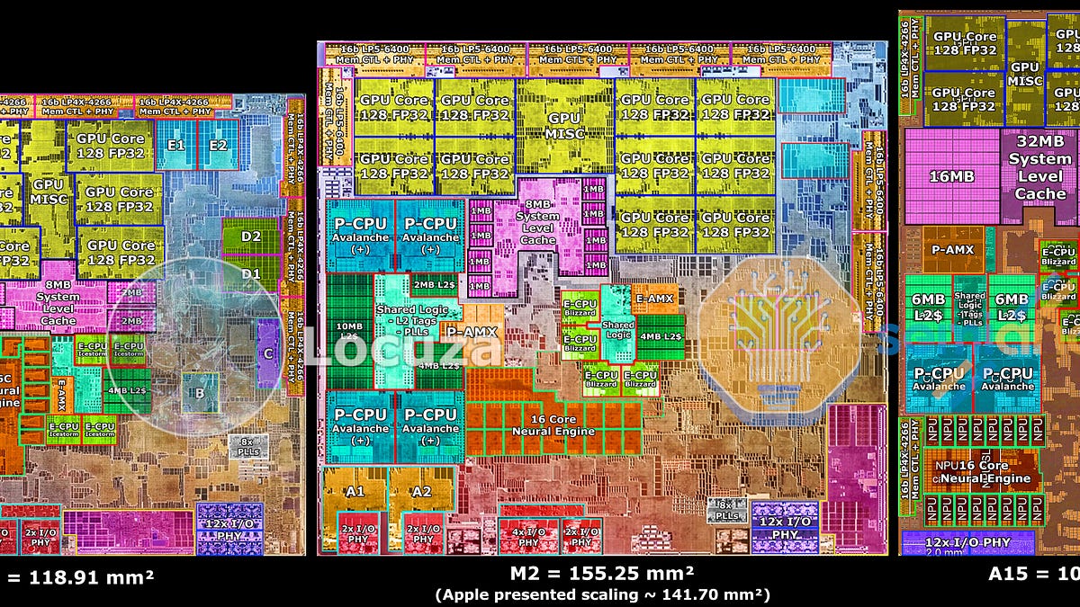
Edit: thanks to Xiao Xi at the other place for tracking M2 figures down:


original source:


Based on this, the M2 Pro's P+E CPU-complex would've been roughly the same size as the Snapdragon Elite's CPU, albeit with 4 smaller E-cores, 2 P-AMX units, 1 E-AMX Unit, and the 8 P-cores being slightly bigger. And a 6% density advantage for the Elite being on N4 vs N5P as I believe N5P has the same density as N5.
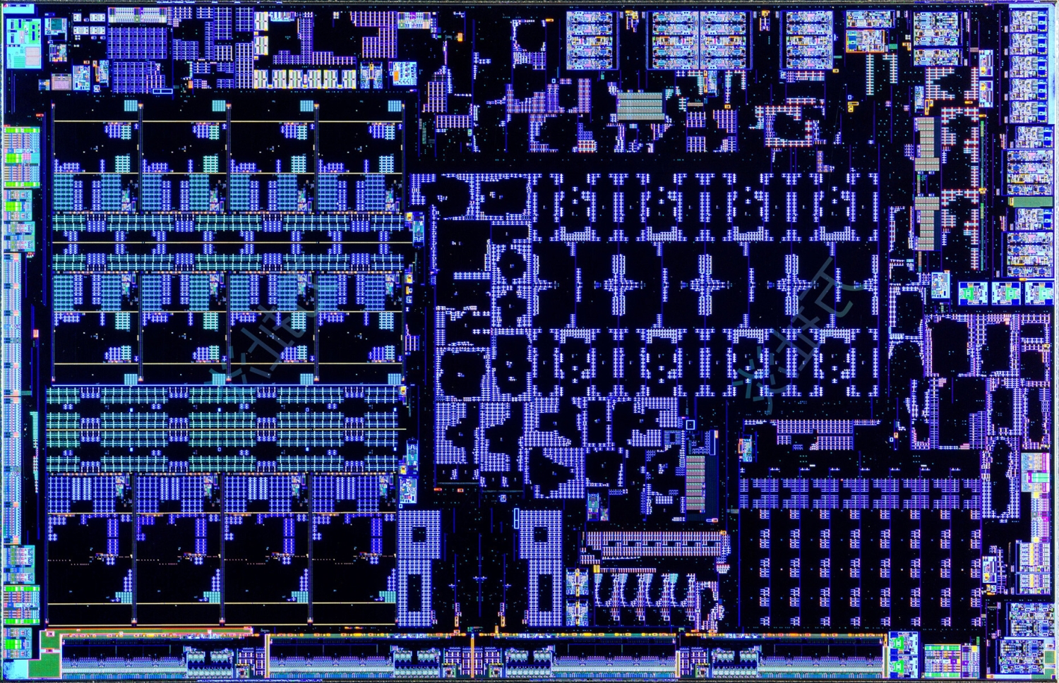
Lunar Lake die shot and size:


Estimate for the Lunar Lake chip based on square pixel area ratios compared to total die area:


all sizes in mm^2"CPU Size"Die
Lunar Lake31.6140
Apple M422.7-27*165.9
*The numbers on the M4 die shot don't add up - the die shot claims that the Apple M4 CPU cluster is 27mm^2 but the sum of each part listed is only 22.7mm^2 - possibly the 27mm^2 is counting the AMX cores which are unhighlighted on the M4 die shot but even that shouldn't be enough to account for the difference (they aren't that big). The same source did the Snapdragon annotation in the above post and the same is not true - the components add up to the total.

While it has a small performance advantage, N3E is slightly less dense than N3B but Lunar Lake has 2.5MB of L2, 3 MB of L3 cache per P-core cluster for a total of 22MB. E-cores have 12MB total of L2 for a total of 34 MB of cache for the CPU which is more than the M4's 20 MB for the CPU. Both have their own SLC, Lunar Lake's is 8MB and I think so the M4's (the M3's definitely is). L1 cache:


L0 cache per coreL1 cache per core (instruction + data)
Lunar Lake48KB P / ?? E64+192 KB P / 64 + 32 KB E
Apple M3-192+128 KB P / 128+64 KB E

Intel has more cache overall with huge L2/L3 for 8 cores like the M4 M3 and similar to the M4’s 10 with two extra E-cores (Edit). And Intel now has actually quite a compact CPU core for a change! The non-L2 die area of the Lion Cove P-core is about 3.2mm^2 vs 3mm^2 for the M4* and 1.12mm^2 for the Skymont E-core vs 0.82 for the M4 E-core with similar amounts of L0 + L1 cache for both P-cores (as of Apple's M3) though Apple's E-core is smaller with (as of M3) double the in-core caches and, again, a slight density advantage for Lunar Lake. But overall Intel has done a really good job creating compact P and E cores and SOC - a far cry from where they were perviously.

*AMD's P-core is about the same as the Intel ~3.2mm^2 with a more pronounced node disadvantage but also less L0/L1 cache per core. Its "c" core is bigger than the Intel E-core but reflects a different design philosophy.
 
Last edited:
“Lol, the recent events make me more convinced than ever that Eric Quinnell knows what he is talking about and uop caches are going the way of Hyperthreading.

Think about it. We had to back off from pipeline stages because adding stages is a guaranteed loss, while prediction is not.

Netburst architectures demonstrated that additional stages cost way more transistors than initially anticipated.

Since the process technologies keep getting better and better still, the idea is to cut the stages again:
-Which improves performance just by itself
-Simplifies design, thus less area and power use, thus more efficient
-Which allows for higher performance by using it elsewhere

Apple has the shortest pipeline at 9. It's that simple.”

Quote from Annadtrch forums.


Is that true @Cmaier ? He says Apple advantage in IPC is because Apple has the shortest pipeline. Where Intel’s skymont has 14 pipelines
I mean the X cores have had short pipelines for a while now (8-10) but only more recently have they somehwat caught up and I think the X925’s IPC will be bolstered partially by 6x128B SIMD in Geekbench tests, without that I expect it the IPC gain (the 15%) is a bit lower, probably 10%. It’s valid of course and somewhat more general than e.g. SME but also kind of straightforward — and not going to aid general integer code as much.

But my point anyway (and the X925 is certainly still going to catch up and be about M3-tier IPC ish) is just that while the shorter pipeline length is helpful — or rather also — the shorter branch misprediction hits (not the same thing but related I think), there’s no way that’s their main performance advantage or source.
 

An unexpected update to an old article I went back to:

Update October 3rd: As expected, the fastes version of the Arc Graphics 140V with a clock of 2.05 GHz is a bit faster than the unit running at 1.95 GHz. However, the test with the new Arc Graphics 140V in combination with the Core Ultra 7 256V should be more interesting for most users, since this SoC is only equipped with 16 GB RAM and only 8 GB are allocated to the iGPU (compared to 16 GB for the 32 GB systems). In addition to the lower power limits, the smaller amount of memory is noticeable and the overall gaming performance is much lower. We need to test more laptops over the next couple of weeks to see how much performance you loose with the 16 GB Lunar Lake CPUs running at higher power limits. If you want to play games on your brand-new Lunar Lake machine, we recommend you get an SoC with 32 GB RAM like the Core Ultra 7 258V.

They're still doing this?! They aren't using true unified memory?! What does the Snapdragon Elite do? Please tell me the CPU/GPU memory split isn't hard coded there too?
 

An unexpected update to an old article I went back to:


They're still doing this?! They aren't using true unified memory?! What does the Snapdragon Elite do? Please tell me the CPU/GPU memory split isn't hard coded there too?
Afaik, while there is one pool of memory, I had always heard it referred to as “shared” rather than unified. Perhaps it’s a lack of knowledge though.
 
Last edited:
They're still doing this?! They aren't using true unified memory?! What does the Snapdragon Elite do? Please tell me the CPU/GPU memory split isn't hard coded there too?

Define "true". It's not clear if this is a fixed split (unlikely) or just an upper limit on how many GPU pages are allowed to exist in memory.

I could have sworn it is absolutely possible to do no-copy ownership transfer of pages between the GPU and CPU on these, unless the newer iGPUs somehow regressed. This isn't really my area.
By true, that's what I mean - allowing both the CPU and GPU to access the same memory with no copy (obviously it would be nice if they also had Nvidia's unified virtual memory pool system but I wasn't referring to that). But why is the upper limit so low? Especially if the memory ownership can be easily swapped? I know Apple has a recommended limit to the amount of GPU memory allocation, but not like this and as I understand it, it is just a recommendation. The wording here is very suggestive of a hard split, but I can see what you're saying about it possibly being just a limit to the number of GPU pages rather than a fixed split. That makes more sense because I too was given to understand that fixed split memory for PC laptops was a thing of the past. Still odd that the limit is apparently so low.
 
By true, that's what I mean - allowing both the CPU and GPU to access the same memory with no copy (obviously it would be nice if they also had Nvidia's unified virtual memory pool system but I wasn't referring to that). But why is the upper limit so low? Especially if the memory ownership can be easily swapped? I know Apple has a recommended limit to the amount of GPU memory allocation, but not like this and as I understand it, it is just a recommendation. The wording here is very suggestive of a hard split, but I can see what you're saying about it possibly being just a limit to the number of GPU pages rather than a fixed split. That makes more sense because I too was given to understand that fixed split memory for PC laptops was a thing of the past. Still odd that the limit is apparently so low.

Again, this is me trying to drag something out of my brain's long term storage, but I could swear that Intel's limits for GPU pages has been in the 50% range for a while.

Instead of expecting a third party to be precise in their language, we can go to Intel and Microsoft's pages on the topic itself: https://www.intel.com/content/www/us/en/support/articles/000020962/graphics.html

It's not clear if this is a Windows limit, or Intel, but since the HD 5300 (2014), this has been the case.
 
From what I understand that is an OS limitation. Intel offers APIs to convert regular allocations to GPU-accessible ones (much like Apple does), no idea whether those also count towards this limit. I wonder what happens if one tries to allocate more.

Apple doesn't seem to have a practical GPU memory limit — I had no trouble allocating buffers much larger than the system RAM size. Metal reports a value documented as "maximal recommended allocation size that won't affect performance", which on my machine is around 75% of the total RAM.

Edit: see post #76 for more details, you can allocate very large buffers, but you can't actually bind more than 75% of total RAM worth of data in a single pass.
 
Last edited:
From what I understand that is an OS limitation. Intel offers APIs to convert regular allocations to GPU-accessible ones (much like Apple does), no idea whether those also count towards this limit. I wonder what happens if one tries to allocate more.

Apple doesn't seem to have a practical GPU memory limit — I had no trouble allocating buffers much larger than the system RAM size. Metal reports a value documented as "maximal recommended allocation size that won't affect performance", which on my machine is around 85% of the total RAM.
Wait you're allowed to allocate such a large GPU buffer it floods into swap? Can you actually write/read to/from that?
 
Wait you're allowed to allocate such a large GPU buffer it floods into swap? Can you actually write/read to/from that?

There are some caveats. I just did a quick test to make sure.

- There is a practical limits to a single buffer size, around 20GB on my system. You only get an error when you try to use it, not at allocation time
- The working size of resident GPU memory cannot exceed the total RAM amount. E.g. if you attempt to access 32GB worth of buffers in a single compute pass, you will get an "out of memory" runtime failure
- You *can* however use more than total RAM worth of buffers in separate compute passes. I had no problem writing to 80GB worth of buffers on my 36GB machine as long as I did not bind more than 27GB worth of data per pass. I suppose the system will swap between passes as needed.

Overall, it appears that the actively accessed GPU data needs to be resident in RAM at all time. The system will swap data in and out as needed. The GPU command submission serves as a boundary for residency management. But it does not seem as if the GPU can currently interrupt execution to swap data in and out. And even if it can, it won't (which is understandable, the performance would be very bad).

There are also sparse resources, which might add an additional dimension to all this, but I don't have experience working with them.

P.S. I also managed to hard freeze my laptop by trying to sequentially process multiple 20+GB buffers. I suppose it hit a slow path in the GPU firmware and the machine reset after a timeout. It was completely unresponsive for a minute or two. I previously had a similar experience experimenting with the texture count limits. It seems like Apple engineers don't expect one to do dumb stuff like that (and who would blame them).
 
Last edited:
There are some caveats. I just did a quick test to make sure.

- There is a practical limits to a single buffer size, around 20GB on my system. You only get an error when you try to use it, not at allocation time
- The working size of resident GPU memory cannot exceed the total RAM amount. E.g. if you attempt to access 32GB worth of buffers in a single compute pass, you will get an "out of memory" runtime failure
- You *can* however use more than total RAM worth of buffers in separate compute passes. I had no problem writing to 80GB worth of buffers on my 36GB machine as long as I did not bind more than 27GB worth of data per pass. I suppose the system will swap between passes as needed.

Overall, it appears that the actively accessed GPU data needs to be resident in RAM at all time. The system will swap data in and out as needed. The GPU command submission serves as a boundary for residency management. But it does not seem as if the GPU can currently interrupt execution to swap data in and out. And even if it can, it won't (which is understandable, the performance would be very bad).

There are also sparse resources, which might add an additional dimension to all this, but I don't have experience working with them.
Awesome. Thanks for the info. Wild stuff. Back when M1 had just released there was a metal bug where allocating more than 2G would silently fail and give you an n mod 2G buffer where n is your requested allocation. Oh how things have improved :D
 
Awesome. Thanks for the info. Wild stuff. Back when M1 had just released there was a metal bug where allocating more than 2G would silently fail and give you an n mod 2G buffer where n is your requested allocation. Oh how things have improved :D

Yeah, I think lack of communication and transparency is the biggest hurdle when working with Apple stuff. The quality of Metal implementation did seem to increase dramatically in the last few years.
 
Overall, it appears that the actively accessed GPU data needs to be resident in RAM at all time. The system will swap data in and out as needed. The GPU command submission serves as a boundary for residency management. But it does not seem as if the GPU can currently interrupt execution to swap data in and out. And even if it can, it won't (which is understandable, the performance would be very bad).

If I understand this correctly, this seems very reasonable, but also elegant. It sounds like the kernel can help coordinate swapping in pages prior to issuing the GPU command as the set of buffers is known at this point. I’d expect normal memory management applies for swapping out. Pages in-use would simply be locked and could not be evicted, but once the GPU commands that rely on them complete, they could be unlocked and marked as eligible for eviction.
 
Hmmm … the next time someone argues that Apple puts the RAM on package because they are cheap:


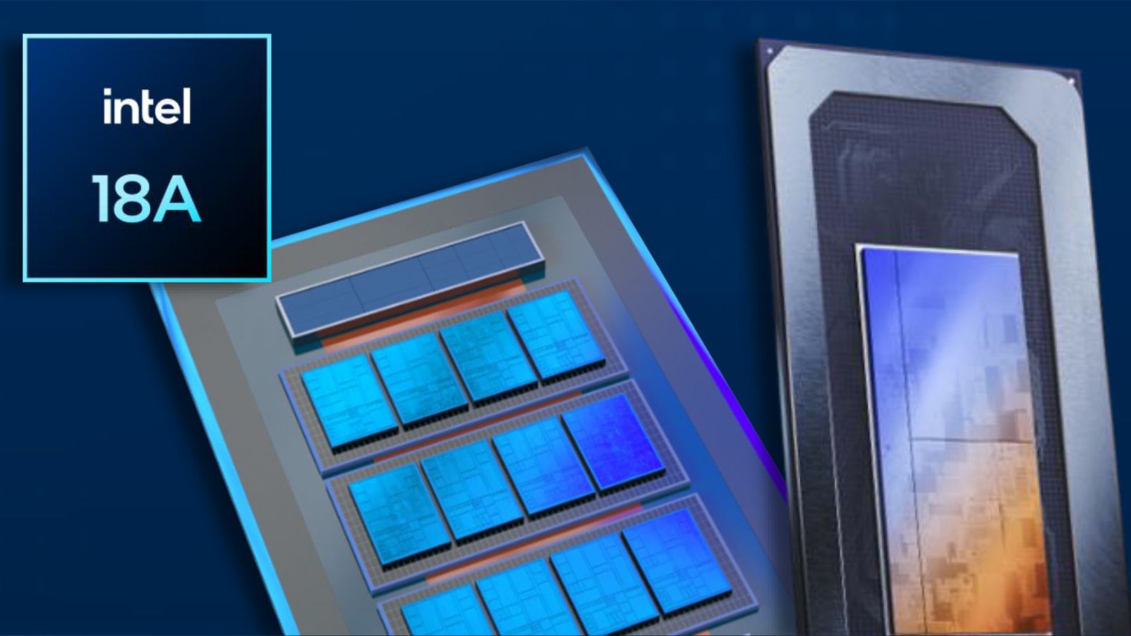
Relatedly, Intel is planning to get off TSMC, but won’t be able to completely do it for the first batch of Intel’s 18A processors (30% will still be TSMC), indicating to me low volume at first. Perhaps expected but it’s important to remember Intel’s need for 18A to be profitable comes not from manufacturing its own chips but being able to serve third parties.

 
Back
Top