I came across this tweet a few days ago that I thought was pretty interesting, seeing as Sumit Gupta leads Apple Cloud Infra products: https://x.com/sumitgup/status/1790875968594432099?s=12I’ve been thinking a lot about M4, Apples move to provide more ‘AI’ as well as rumours of Apple building out large data centres with Apple silicon derived hardware to power their own machine learning efforts.
It got me to thinking that at WWDC I wouldn’t be surprised if they announce availability of Apple Silicon in the cloud for developers too for machine learning purposes - they already support XCode cloud for CI/CD, build and testing on Apple devices. Might/Could be a natural evolution of the service and certainly another area that they can slap that big upselling buzzword (‘AI’) to drive up the stock price!
It also got me to thinking about M4 and the ability for Apple to offer data centers for more Apple specific app services in the cloud such as Final Cut Pro (e.g. offline rendering, generation of proxies etc… following the asyncronous ‘compute rental model’.
When you think about how compute dense and capable Apple Silicon is at such low power requirements - with M4 coming now with capable vector processing, a very capable power sipping GPU, very capable media decode and encode engines etc… as well as the small areas that such chips can fit within, I do think its’ a no brainer for Apple to build out some of their own data centers to power more Apple Services.
Given fast interconnect, I can’t see why a rack of M4 XServes wouldn’t be a very attractive offering when you compare to the power and cooling requirements of AMD EPYC and Intel Xeon
You are using an out of date browser. It may not display this or other websites correctly.
You should upgrade or use an alternative browser.
You should upgrade or use an alternative browser.
SME in M4?
- Thread starter jbailey
- Start date
I got my M4 and was able to spend a couple of hours playing with SME today. I get 250 GFLOPs for the single-precision vector streaming mode. As I suspected, it makes a difference whether one uses the base SVE instruction that accumulates to the SVE registers or the new SME2 instruction that accumulates to the matrix storage. This is why my result is x8 higher than what the other team has reported. Not too shabby for a passively cooled tablet. One can probably go faster if one uses multiple threads, I'll have to try it out.
Also, it took me a lot of effort to figure out how SME instructions work. Admittedly, it's been a while since I last touched assembly, but SME is particularly complex and I don't feel that the manual does a good job explaining the concepts at all. Some examples would do wonders. The layout of the SME tile storage is particularly difficult to follow, and not intuitive at all. I do see why they designed it this way though: it's the best way to accommodate hardware with different vector sizes.
Also, it took me a lot of effort to figure out how SME instructions work. Admittedly, it's been a while since I last touched assembly, but SME is particularly complex and I don't feel that the manual does a good job explaining the concepts at all. Some examples would do wonders. The layout of the SME tile storage is particularly difficult to follow, and not intuitive at all. I do see why they designed it this way though: it's the best way to accommodate hardware with different vector sizes.
- Joined
- Nov 29, 2021
- Posts
- 563
I'd love some elaboration on this or references to better sources than the official manual if you found any.Also, it took me a lot of effort to figure out how SME instructions work. Admittedly, it's been a while since I last touched assembly, but SME is particularly complex and I don't feel that the manual does a good job explaining the concepts at all. Some examples would do wonders. The layout of the SME tile storage is particularly difficult to follow, and not intuitive at all. I do see why they designed it this way though: it's the best way to accommodate hardware with different vector sizes.
You can't get clang to emit SME?
I'd love some elaboration on this or references to better sources than the official manual if you found any.
It was mostly trial and error for me, and fumbling around intrinsics with compiler explorer.
You can't get clang to emit SME?
Maybe one has to find the right combination of flags. Assembly worked for me. The intrinsics are not very transparent, but now that I understand the assembly I think I start getting the intrinsics too.
One has to keep in mind that this is incredibly new and niche tech. Even for SVE there are very few resources, and that has been around for a while.
- Joined
- Nov 29, 2021
- Posts
- 563
Sure. What about Accelerate though. I assume it’s a safe bet it will dispatch to SME where available?It was mostly trial and error for me, and fumbling around intrinsics with compiler explorer.
Maybe one has to find the right combination of flags. Assembly worked for me. The intrinsics are not very transparent, but now that I understand the assembly I think I start getting the intrinsics too.
One has to keep in mind that this is incredibly new and niche tech. Even for SVE there are very few resources, and that has been around for a while.
Sure. What about Accelerate though. I assume it’s a safe bet it will dispatch to SME where available?
Accelerate still works and is probably as fast as ever
")
You're not alone! I've had a skim through DDI 0487K.a (which I believe is the latest version of the Armv8/9 architecture spec) trying to understand SME and it's tough. The SME material is pure specification-ese with no thought given to making it approachable.Also, it took me a lot of effort to figure out how SME instructions work. Admittedly, it's been a while since I last touched assembly, but SME is particularly complex and I don't feel that the manual does a good job explaining the concepts at all. Some examples would do wonders. The layout of the SME tile storage is particularly difficult to follow, and not intuitive at all. I do see why they designed it this way though: it's the best way to accommodate hardware with different vector sizes.
Granted, an architecture manual needs to be specifications first, but just a few paragraphs of non-binding introductory description here and there works wonders. I haven't found this doc this hard to read when trying to understand other things about Armv8/9.
Moving the discussion over here since I think it fits better. It is odd that the leak/rumor mill points to AMD using "true" AVX-512 in Zen 5. Their Zen 4 implementation seems really performant already and I am concerned that chasing pure performance in those workloads could lead them down the same bad paths as Intel with respect to heat. That said, so far, AMD CPU engineers have shown that they know what they are doing. So if they are going down this road, I'm more confident that they'll do it right.Zen4's AVX512 Teardown - mersenneforum.org
Embargo has lifted! So here's that teardown I've promised! I won't get into how this happened, but AMD graciously sent me two test setups this year. A retail Zen3 setup back in January, and an engineering Zen4 setup in August. The motivation here is to let me optimize y-cruncher for these...www.mersenneforum.org
“But anyway, we live in a very strange world now. AMD has AVX512, but Intel does not for mainstream... If you told me this a few years ago, I'd have looked at you funny. But here we are... Despite the "double-pumping", Zen4's AVX512 is not only competitive with Intel's, it outright beats it in many ways. Intel does remain ahead in a few areas though.”
from another place:
“Zen4 AVX512 is mostly double-pumped: a 256-bit native hardware that processes two halves of the 512-bit register.”
So they saved area and complexity (they have four total 256-bit units but for different purposes each) along with power and just double pumped but still found a way to beat Intel’s original, hotter implementation of AVX-512. It’s a pretty great implementation.
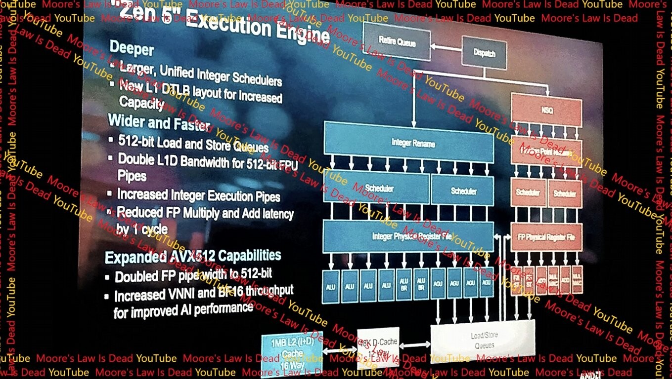
AMD Zen 5 Execution Engine Leaked, Features True 512-bit FPU
AMD "Zen 5" CPU microarchitecture will introduce a significant performance increase for AVX-512 workloads, with some sources reported as high as 40% performance increases over "Zen 4" in benchmarks that use AVX-512. A Moore's Law is Dead report detailing the execution engine of "Zen 5" holds the...
This is also the first time that I've seen the 40% increase in performance number floating around for Zen 5 specifically referencing to an increase in AVX-512 workloads. Previous articles and ... uhhh ... certain individuals made it sound like a more general increase in FP/Int performance. I'm not going to dismiss a 40% increase in those workloads mind you any more than I would for SME*. As long as power is kept under control, it's important to pursue gains wherever they can be made.
Of course these are all leaks and rumors so everything from numbers to even the AVX design should be taken with a mound of salt rather than the grain accompanying official pre-release figures.
*I won't hold my breath for those that did dismiss results due to SME to apply the same standards to AMD improving AVX-512 if indeed that is where the biggest gains come from.
Here is my initial round of microbenchmarks for the M4 SME unit, for those who are interested:

 github.com
Feedback and contributions are welcome!
GitHub - tzakharko/m4-sme-exploration: Exploring the scalable matrix extension of the Apple M4 processor
Exploring the scalable matrix extension of the Apple M4 processor - tzakharko/m4-sme-exploration
github.com
Feedback and contributions are welcome!
Very cool! About latency: communication of the CPU with the SME unit should be faster than going to the NPU no? After all, the SME unit communicates through L2 but the NPU/GPU only share the SLC/L3 with the CPU - is that rightt? (and of course RAM, but yeah ...)Here is my initial round of microbenchmarks for the M4 SME unit, for those who are interested:
GitHub - tzakharko/m4-sme-exploration: Exploring the scalable matrix extension of the Apple M4 processor
Exploring the scalable matrix extension of the Apple M4 processor - tzakharko/m4-sme-exploration
Feedback and contributions are welcome!
Very cool! About latency: communication of the CPU with the SME unit should be faster than going to the NPU no? After all, the SME unit communicates through L2 but the NPU/GPU only share the SLC/L3 with the CPU - is that rightt? (and of course RAM, but yeah ...)
That’s my understanding as well. Even more, there has to be a fast command transfer channel between the cores and the SME unit since the instructions come from the CPU and refer to parts of the CPU state (such as base indexing register for selecting ZA slices)
One thing I'd like to see, and this is more something for Apple to provide truthfully, is an optimization guide, similar I suppose to what Apple released for the CPU that @Jimmyjames shared, but not just for the SME performance detailing what you've done here, but even more broadly vector/matrix/AI processing on NEON/SME/NPU/GPU. Addressing the gestalt of all the options and the interplay between them. In other words, a thorough description or guideline about what kinds of workloads, and how big, should be used for each processor type: what is the latency of different job types to each, what units can really cooperate tightly together (as you mentioned the SME and NEON units), what are the programming implications of how to set up your workloads, etc ... I know that CoreML right now doesn't let you necessarily target a particular processor*, but we'll see come WWDC what the state of play is on that and beyond that, now that the SME unit can be targeted directly with extensions, I feel like it could be useful for developers to get a sense of how Apple views the purpose of each unit and what to expect from them. Maybe they have something like this already or in the works.That’s my understanding as well. Even more, there has to be a fast command transfer channel between the cores and the SME unit since the instructions come from the CPU and refer to parts of the CPU state (such as base indexing register for selecting ZA slices)
*well it kinda does right? I believe you can suggest which accelerator you would like, but it just isn't guaranteed to go there or stay there. Like with CPU threads the OS reserves the right to redirect. That's my base understanding anyway.
- Joined
- Nov 29, 2021
- Posts
- 563
Dude, this is wild work already. It may not be that much code, but having to do the research required to write this in the time the M4 has been out is pretty impressive. Almost feel like we should be paying you for these insightsHere is my initial round of microbenchmarks for the M4 SME unit, for those who are interested:
GitHub - tzakharko/m4-sme-exploration: Exploring the scalable matrix extension of the Apple M4 processor
Exploring the scalable matrix extension of the Apple M4 processor - tzakharko/m4-sme-exploration
Feedback and contributions are welcome!
")
Did you look much into the proprietary AMX instruction set? Is it gone from M4 or does it still work? Does it seem that the ARM SME set here maps 1:1 to Apple's prior AMX instructions?
Do you have any insights into the cost of being in a startsme block? It seems it adds cost to context switches until you "stopsme" as the hardware accelerator's state needs to be restored after context switches
This is awesome. Thanks dudeHere is my initial round of microbenchmarks for the M4 SME unit, for those who are interested:
GitHub - tzakharko/m4-sme-exploration: Exploring the scalable matrix extension of the Apple M4 processor
Exploring the scalable matrix extension of the Apple M4 processor - tzakharko/m4-sme-exploration
Feedback and contributions are welcome!
Dude, this is wild work already. It may not be that much code, but having to do the research required to write this in the time the M4 has been out is pretty impressive. Almost feel like we should be paying you for these insights
Haha, thanks for the kind words! It wasn’t that much work though, really, just a little weekend project. The tests themselves are very simple. The difficult part was figuring out the instruction formats and semantics. Then I used a simple script to generate the benchmarks themselves.
Did you look much into the proprietary AMX instruction set? Is it gone from M4 or does it still work? Does it seem that the ARM SME set here maps 1:1 to Apple's prior AMX instructions?
I didn’t test any AMX instructions. SME seems much more complex than the instruction set described by corsix to me, but that’s just an impressionistic judgement.
Do you have any insights into the cost of being in a startsme block? It seems it adds cost to context switches until you "stopsme" as the hardware accelerator's state needs to be restored after context switches
How would you test this? Sounds really complicated. I only did very simple things, didn’t even measure latency.
- Joined
- Nov 29, 2021
- Posts
- 563
No clue. It's pretty hard without tapping into the kernel's task scheduler I think. If we had a macOS device, it might be possible to build a custom XNU where it could be done, but I think all but impossible on iOS/iPadOS. - I welcome ideas though and hoped you might have someHow would you test this? Sounds really complicated. I only did very simple things, didn’t even measure latency.

Jimmyjames
Elite Member
- Joined
- Jul 13, 2022
- Posts
- 1,507
In case anyone hasn’t seen it, here is Geekerwan’s M4 iPad video, with various technical details. It really does like a nice IPC increase.
In case anyone hasn’t seen it, here is Geekerwan’s M4 iPad video, with various technical details. It really does like a nice IPC increase.
Interesting that from the GPU tests he is concluding that (contrary to all the people calling N3B a big failure) that the N3E process doesn't bring much in the way of perf/watt improvements.
My interpretation of the video is that with LN cooling the base M4 now seems to top out at 30W and in the iPad (without LN) it tops out at 14W or so. Certainly bodes well for the less thermally constrained Macs that we should get later this year.
Also remarkable that the CPU changed so much.
Edit: Should also add that based on his conclusions the N3E process brings higher frequency ceilings but while that may be true I don't know if we can determine the ratio of frequency improvement of the M4 are due to N3E vs the improvement due to changes in the microarchitecture.
Last edited:
- Joined
- Sep 26, 2021
- Posts
- 8,274
- Main Camera
- Sony
i always assumed that it was more a yield thing than a performance thing (N3E). Could also be that they laid things out so as to be compatible with both processes, and didn’t take full advantage (I did that once or twice).Interesting that from the GPU tests he is concluding that (contrary to all the people calling N3B a big failure) that the N3E process doesn't bring much in the way of perf/watt improvements.
My interpretation of the video is that with LN cooling the base M4 now seems to top out at 30W and in the iPad (without LN) it tops out at 14W or so. Certainly bodes well for the less thermally constrained Macs that we should get later this year.
Also remarkable that the CPU changed so much.
Edit: Should also add that based on his conclusions the N3E process brings higher frequency ceilings but while that may be true I don't know if we can determine the ratio of frequency improvement of the M4 are due to N3E vs the improvement due to changes in the microarchitecture.
In case anyone hasn’t seen it, here is Geekerwan’s M4 iPad video, with various technical details. It really does like a nice IPC increase.
Interesting that he says the higher bandwidth comes from LPDDR5-7500 rather than (as most, including he, thought) LPDDR5X-7500. He says they chose the former for latency reasons, implying LPDDR5-7500 would have better latency than LPDDR5X-7500. He may say more about this later, but i haven't had a chance to view the whole thing.
He also posted SPEC 2017 P-core (single-core) results. [I don't think these are with LN, but I'm not certain.] He says that the improvement between M3 and M4 with SPEC (+19%) is similar to that seen with GB5 (+17%). With GB6.3, the addition of SME support enables the M4 to pull ahead more (+23%).
And here's a P-core comparison of the M3 and M4 to the 6.0 GHz i9-14900K. The percentages are M4/i9-100:
Last edited: