M2 Pro and M2 Max

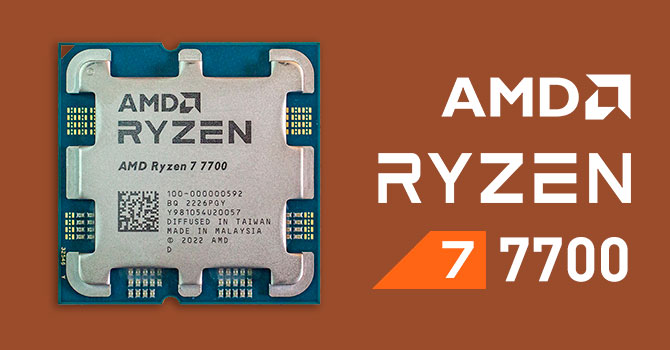
From this I can say that the M2 Max is on par with Ryzen 7 7700 (8 Core) Zen 4. The non-X variant uses 90 Watts maximum at stock setting.( You can OC it but demimishing returns and power usage increases) so best to stay at stock.
....
I can say AMD and Apple use of TSMC 5nm is good. Both efficient parts and these parts are very good to use in micro/mini ATX towers.

......

EDIT: When I mean 90 Watts max, it's like apps like blender. Gaming and normal apps obviously don't use 90 watts its much lower than that.
90W max with Blender means CPU+GPU.

What's the Ryzen 7700's max wattage for CPU only (it's nominally 65W), and how does that compare with the M2 Max's? I suspect when the M2 Max's figures come out, they will be substantially lower, indicating they are not similar in efficiency.

And for CPU + GPU, I assume the processors are not comparable—I'd expect the GPU on the M2 Max to be substantially more powerful than that the integrated GPU that comes with the 7700 (according to one GB result I saw, it's an RX Vega 2). So if you want to compare the AMD's offerings with the M2 Max for CPU + GPU efficiency, you'd need to look at the wattage of the 7700 plus whatever AMD discrete GPU is needed to equal the performance of the M2 Max.
 
Last edited:
90W max with Blender means CPU+GPU.

What's the Ryzen 7700's max wattage for CPU only (it's nominally 65W), and how does that compare with the M2 Max's? I suspect when the M2 Max's figures come out, they will be substantially lower, indicating they are not similar in efficiency.

And for CPU + GPU, I assume the processors are not comparable—I'd expect the GPU on the M2 Max to be substantially more powerful than that the integrated GPU that comes with the 7700 (according to one GB result I saw, it's an RX Vega 2). So if you want to compare the AMD's offerings with the M2 Max for CPU + GPU efficiency, you'd need to look at the wattage of the 7700 plus whatever AMD discrete GPU is needed to equal the performance of the M2 Max.
No you can also do CPU only tests in blender. This does not include the GPU and Zen 4(7000 series) uses RDNA 2 IP but that's mostly for basiv monitor connectivity as these are desktop chips.

AMD also has their mobile line of Zen 4 CPUs which are far more efficient as they are monolithic and they have much better iGPUs. Will be interesting to see the efficiency gains.

This video explains the 88 watt desktop parts from AMD
 
No you can also do CPU only tests in blender. This does not include the GPU and Zen 4(7000 series) uses RDNA 2 IP but that's mostly for basiv monitor connectivity as these are desktop chips.
OK, I confirmed that the peak CPU package power for the 7700 is 90 W on anandtech:

And for the M1 Max, anandtech says the peak CPU package power is 43W:
Let's assume that, at most, the peak CPU package power for the M2 Max is 20% higher (it may not be that much, but let's give the 7700 a fighting chance). That's 52W.

Using GB scores, the MT efficiency of the 7700 is 13500 points/90 W ≈ 150 points/W
And the minimum projected MT efficiency of the M2 Max is 15200 points/52 W ≈ 290 points/W

And 290/150 ≈ 2, so I project the M2 Max is about twice as efficient as the Ryzen 7700.

I thus disagree with this characterization, which paints them as comparable:
I can say AMD and Apple use of TSMC 5nm is good. Both efficient parts and these parts are very good to use in micro/mini ATX towers.
 
And 290/150 ≈ 2, so I project the M2 Max is about twice as efficient as the Ryzen 7700.
Peak package power would have to include the M2 Max's 38 core GPU, as opposed to whatever the 7700 would be using on-board/slot to accomplish the same result. The 7700 has two graphics cores, because … because … um … reasons?
 
Peak package power would have to include the M2 Max's 38 core GPU, as opposed to whatever the 7700 would be using on-board/slot to accomplish the same result. The 7700 has two graphics cores, because … because … um … reasons?
Take a look at the article I referenced. You'll see that the 43W figure I quoted was for the M1's peak package power under CPU-only loads ("In multi-threaded scenarios, the package and wall power vary from 34-43W on package, and wall active power from 40 to 62W"). They report "stressing out both CPU and GPU at the same time, the SoC goes up to 92W package power"
 
Take a look at the article I referenced. You'll see that the 43W figure I quoted was for the M1's peak package power under CPU-only loads ("In multi-threaded scenarios, the package and wall power vary from 34-43W on package, and wall active power from 40 to 62W"). They report "stressing out both CPU and GPU at the same time, the SoC goes up to 92W package power"
While I think your general ideas are good and that the M series is more efficient I question whether Geekbench approaches the peak package power on either and whether we can really use it with a peak power draw figure like that. I think an average draw throughout the test would be significantly better but of course also harder to come by data wise. But AMD. AMD may give its peak value in AVX workloads or something and regular operating wattage be significantly lower.

On the other hand does the M package power you consider here include memory since it’s on package? And other potential parts that are on die on M but on separate chipset components on AMD? It wouldn’t account for much since it would be power gated but it could still be a watt or two.
 
While I think your general ideas are good and that the M series is more efficient I question whether Geekbench approaches the peak package power on either and whether we can really use it with a peak power draw figure like that. I think an average draw throughout the test would be significantly better but of course also harder to come by data wise. But AMD. AMD may give its peak value in AVX workloads or something and regular operating wattage be significantly lower.
These are reasonable concerns, and to address them you'd need to see if the relative GB MT scores are reflective of the relative performance with CPU-only tasks that have been shown to draw peak power, and are equally optimized for AMD and AS (my analysis assumes they are)--or to determine the relative CPU package wattage for GB MT; or to look at average wattage and performance values for sustained workloads (again, using CPU-only tasks that are equally optimized for AMD and AS). I leave these for you to pursue if you wish ;).
On the other hand does the M package power you consider here include memory since it’s on package? And other potential parts that are on die on M but on separate chipset components on AMD? It wouldn’t account for much since it would be power gated but it could still be a watt or two.
I was looking for a coarse-grained estimate, and if the efficiency difference really is about two-fold, I think these effects can be ignored.
 
Using GB scores, the MT efficiency of the 7700 is 13500 points/90 W ≈ 150 points/W
And the minimum projected MT efficiency of the M2 Max is 15200 points/52 W ≈ 290 points/W

And 290/150 ≈ 2, so I project the M2 Max is about twice as efficient as the Ryzen 7700.

I thus disagree with this characterization, which paints them as comparable:
The Ryzen 9 7900 is even more efficient than the 7700 due having more cores and thus lower base clocks.

Also I never said AMD desktop parts are more efficient than Apple's. AMD's chiplet design is not made for efficiency but scaling (The IO die is also 6nm which also increases power).
Their laptops parts however are monolithic(like the M series) should offer efficiency close the M2 Max/Pro.

Techpowerup did good review on AMD Ryzen 7700:

It averages 57.8watts in apps.

1674709414905.png


Same in games as well:
1674709476950.png


*sigh* I wish we got graphs like this from the likes of Mac reviewers.

techpowerup has very detailed reviewers/articles.
 
Last edited:
Also I never said AMD desktop parts are more efficient than Apple's. AMD's chiplet design is not made for efficiency but scaling (The IO die is also 6nm which also increases power).
Their laptops parts however are monolithic(like the M series) should offer efficiency close the M2 Max/Pro.

Just a small point: Back when the IO die was GloFo 14nm that caused a large amount of excess power draw even in idle - it certainly got the blame for it in most of the reviews of previous generation chips, believably I would say. However at 6nm, the difference between that and a monolithic 4nm should be negligible as IO die structures simply don’t scale very well and the scaling for the IO structures relative to logic gets worse the smaller you get.
 
Just a small point: Back when the IO die was GloFo 14nm that caused a large amount of excess power draw even in idle - it certainly got the blame for it in most of the reviews of previous generation chips, believably I would say. However at 6nm, the difference between that and a monolithic 4nm should be negligible as IO die structures simply don’t scale very well and the scaling for the IO structures relative to logic gets worse the smaller you get.
It still has an impact even at 6nm because Intel's monolithic 13th gen CPUs draw less power when idle than 5nm Zen 4 desktop CPUs and also keep in mind that Intel is stuck on Intel 7++++
 
It still has an impact even at 6nm because Intel's monolithic 13th gen CPUs draw less power when idle than 5nm Zen 4 desktop CPUs and also keep in mind that Intel is stuck on Intel 7++++
I dunno I watched a gamer’s nexus video which was actually an AMD presentation on the subject (mostly in relation to the GPU but it should hold for the CPU too) and AMD were pretty adamant that the difference was pretty negligible going from 6 to 5 (and even lower!) makes almost no difference to IO die power draw or structure size.


This is not the first time I’ve seen this - of course often it’s in relation to SRAM/cache on the CPU but IO sounds even worse. I mean I’m sure there’s some logic on the IO die that does benefit but apparently a lot of it doesn’t. We’ll see when the monolithic parts come out.
 
Last edited:
I dunno I watched a gamer’s nexus video which was actually an AMD presentation on the subject (mostly in relation to the GPU but it should hold for the CPU too) and AMD were pretty adamant that the difference was pretty negligible going from 6 to 5 (and even lower!) makes almost no difference to IO die power draw or structure size.


This is not the first time I’ve seen this - of course often it’s in relation to SRAM/cache on the CPU but IO sounds even worse. I mean I’m sure there’s some logic on the IO die that does benefit but apparently a lot of it doesn’t. We’ll see when the monolithic parts come out.


this reddit thread shows otherwise, it think its the chiplet design. No wonder AMD does monolithic designs for laptops.
 

this reddit thread shows otherwise, it think its the chiplet design. No wonder AMD does monolithic designs for laptops.

Hmmm the one Redditor on there with a theory said it was indeed the chiplet design but *not* the fabrication node. Rather the power between chiplets is always on.


That would indicate that if you were to keep AMDs chiplet design but move the IO die to 5nm then nothing would change. The idle power draw would still be bad. I wonder how testable that is and AMD could do to fix that if so. Edit: To some extent it makes sense. Even for logic the power used by 5nm doesn’t go down by as much from 6nm as what is being claimed for AMD’s idle power draw vs monolithic.

Has anyone looked at the Ultra’s idle power draw relative to the Max’s? It would be an interesting point of comparison if Apple’s design suffers the same … or doesn’t.
 
Last edited:
Hmmm the one Redditor on there with a theory said it was indeed the chiplet design but *not* the fabrication node. Rather the power between chiplets is always on.


That would indicate that if you were to keep AMDs chiplet design but move the IO die to 5nm then nothing would change. The idle power draw would still be bad. I wonder how testable that is and AMD could do to fix that if so.

Has anyone looked at the Ultra’s idle power draw relative to the Max’s? It would be an interesting point of comparison if Apple’s design suffers the same … or doesn’t.

Yeah I saw that. Also I googled the idle power draw on a 13th gen Intel CPU.

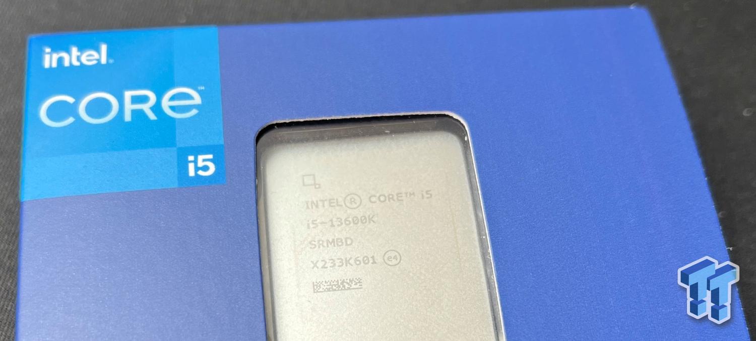
The 7600X idles at 18 watts more than the i5 13600k which is only 6 watts.
The i9 13900k idles at 10 watts while AMD's 7950X idles at 24 watts.

1674713793368.png


I believe Apple will never use chiplets is efficiency and idle power draw is important for them.
 
Yeah I saw that. Also I googled the idle power draw on a 13th gen Intel CPU.

The 7600X idles at 18 watts more than the i5 13600k which is only 6 watts.
The i9 13900k idles at 10 watts while AMD's 7950X idles at 24 watts.

View attachment 21529

Yeah it’s not the node then as I wrote above in an edit even logic doesn’t gain that much efficiency from 6nm to 5nm as the stated difference between AMD’s chiplet vs Intel/AMD monolithic designs.
I believe Apple will never use chiplets is efficiency and idle power draw is important for them.

Except that Apple’s Ultra chip essentially is a chiplet design. It’s just Apple’s take on it and I wonder if their ultra fusion connector (really TSMC’s I think) is somehow more efficient than AMD’s solution (which I suspect now is using something similar as they should have access to TSMC’s packaging tech too) or something else is at play. Still also trying to figure out if the ultra fusion connector is at the root of Apple’s Ultra GPU scaling woes or something else - even @Andropov ’s theory that most of it is software inefficiency is in play though I still think it’s less likely.
 
Also I never said AMD desktop parts are more efficient than Apple's.
I never said you did. I said you portrayed them as being "comparable" in efficiency:
I thus disagree with this characterization, which paints them as comparable:
...which is what you did:
I can say AMD and Apple use of TSMC 5nm is good. Both efficient parts and these parts are very good to use in micro/mini ATX towers.
So if you can reference a clean comparison showing that any AMD chip is comparable in efficiency to any Apple Silicon chip in the same category (i.e., where both chips are roughly equally performant), I'd be interested to read it.
 
So if you can reference a clean comparison showing that any AMD chip is comparable in efficiency to any Apple Silicon chip in the same category (i.e., where both chips are roughly equally performant), I'd be interested to read it.
We will have to wait till mobile Zen 4 laptops to see really just how efficient AMD designs are for Apples to apples comparisons.
 
Their laptops parts however are monolithic(like the M series) should offer efficiency close the M2 Max/Pro.

For lower-end stuff, where AMD uses 8 cores with very low clocks agains a 4+4 M2, certainly. For higher-powered stuff (like the upcoming 7940HS), I'd expect AMD to use at least 30% more power than M2 Pro for the same performance.
 
Except that Apple’s Ultra chip essentially is a chiplet design. It’s just Apple’s take on it and I wonder if their ultra fusion connector (really TSMC’s I think) is somehow more efficient than AMD’s solution (which I suspect now is using something similar as they should have access to TSMC’s packaging tech too) or something else is at play.
AMD isn't using advanced packaging tech like Apple, just conventional organic substrates. The IFOP (Infinity Fabric On Package) links connecting their Core Complex Die (CCDs) to the IO die are narrow and high clock rate per wire, meaning they require SERDES.

It's a bit harder to be certain about Apple's setup as they give out even less detail than AMD, but the numbers we do have say their interface is very wide and slow. On the one hand, power per bit lane should be way lower with Apple's approach - AMD's packaging means transmission lines are longer and should require a lot more energy to yank around, and needing a SERDES for each wire costs both silicon and power. On the other hand, Apple has a lot more wires in their die-to-die interconnect. I have no great feel for who wins here.

Apple arguably had a tougher problem to solve: they had to make their solution support splitting the GPU in two. In AMD's Zen desktop products, they don't have as large a GPU, and it's always completely contained within the IO die (which is where the memory controllers live), so no need to pollute the IFOP links with GPU traffic. While Apple's GPU cores probably don't need to talk to each other much, they should need to talk to memory attached to the other die quite a bit.

Yet another difference between the two systems is that there is no local DRAM memory controller in a CCD. So, AMD's CPUs always have to go off-die for cache misses, and IFOP links are almost certainly higher latency than Apple's interconnect. The tradeoffs here are just so very different.

As an aside, in this realm, people usually measure in units of picojoules per bit transported from one chip to another. Kind of a neat unit.

Still also trying to figure out if the ultra fusion connector is at the root of Apple’s Ultra GPU scaling woes or something else - even @Andropov ’s theory that most of it is software inefficiency is in play though I still think it’s less likely.
I don't think there's much pure forum posting can do to provide definitive answers. Best approach I can think of is acquiring three M1 systems (pro, max, and ultra), getting real familiar with Metal, and going to town writing microbenchmarks. Wherever you find things which don't scale the same from Pro to Max to Ultra, you can investigate with Apple's performance monitor / counter features, which I've heard are pretty good. Apple provides these tools to enable developers to figure out performance bugs in their code, but they should also be able to provide some amount of insight into why some particular thing doesn't scale as well from Max to Ultra as you'd expect.

My intuition, for what it's worth, is that it probably isn't Ultra Fusion. UF seems intentionally overengineered, as if Apple wanted to make certain that if there were problems scaling their GPU up to be huge, the interconnect wouldn't be one.
 
Back
Top