X86 vs. Arm

Hey guys,

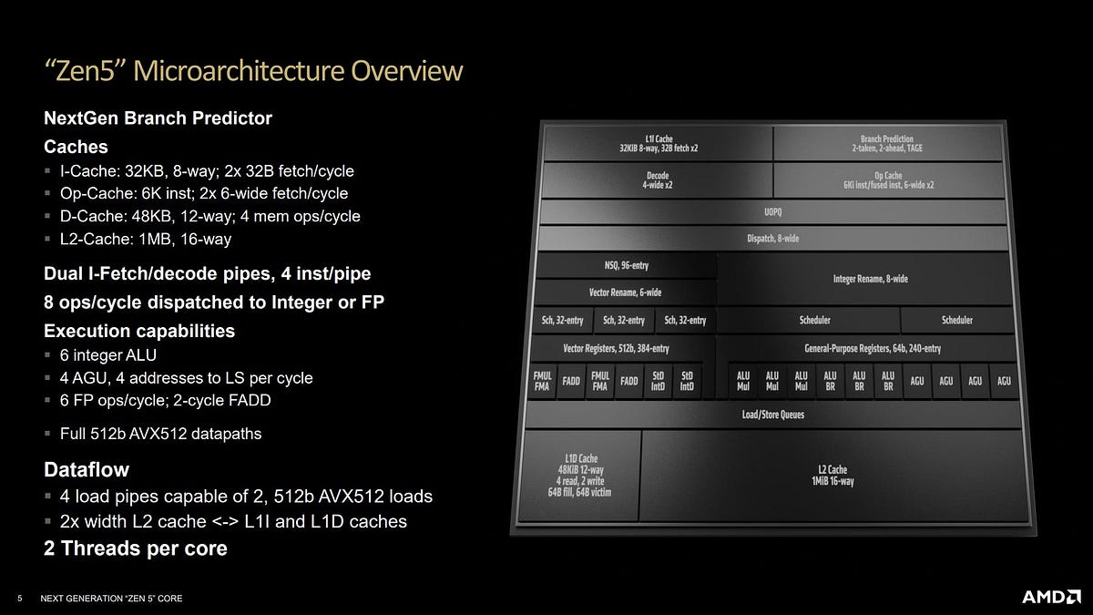
Back with another question. This time about Zen5's dual decoders. We see in the diagram that 1T is limited to 4 instructions, is it the same case for M4?

They use very different approaches to decoding. M4 decodes 10 instructions from a single thread per cycle. If I understand Zen4 correctly, it uses the 4-wide decoders to follow different branch paths. It’s a smart way to improve decode performance without introducing too much complexity or added power consumption. Intel went for a more expensive wide decode design.


I still find it hard to imagine how an x86 machine can have 4-wide decoders when one decoder does not know what to work on before the decoder before it finds the instruction boundary.

There are algorithms that exploit parallel hardware to do sequential work. These algorithms operate in multiple stages, with parallel operations that examine individual elements and pass the results to the next parallel stage. It’s just the wider you want to make these things, the more stages and data pipes you need, and the entire thing becomes exponentially more expensive. You can look at sorting networks for a good example. SIMD UTF8 decode is another good one.
 
There are algorithms that exploit parallel hardware to do sequential work. These algorithms operate in multiple stages, with parallel operations that examine individual elements and pass the results to the next parallel stage. It’s just the wider you want to make these things, the more stages and data pipes you need, and the entire thing becomes exponentially more expensive. You can look at sorting networks for a good example. SIMD UTF8 decode is another good one.
It’s also very power inefficient. You have a lot of circuits doing speculative work, and you throw away a lot of that work.
 
I could see a decoder that looks at the first 4 bytes to attempt to determine where the instruction boundary is and if it can figure it out, passes the next instruction boundary to the second decoder, on down the line, so they are serially parallel, much of the time. I think r/m and sib, if present, will always be adjacent bytes. Hence, it could be parallel-ish for large parts of the instruction stream, if it is compiled well. And, of course, there are two 4-wide decoders because the cores on AMD machines are always dual-thread capable – if the core is only running one thread, the second decoder group is idle.
 
And, of course, there are two 4-wide decoders because the cores on AMD machines are always dual-thread capable – if the core is only running one thread, the second decoder group is idle.

No, they use the two decoders simultaneously even for single-threaded operation - they follow different branches. This is one of major contributors to increased IPC in Zen 5.
 
No, they use the two decoders simultaneously even for single-threaded operation - they follow different branches. This is one of major contributors to increased IPC in Zen 5.
I don't think that's right:


Superficially, Zen 5’s frontend looks like the ones in Intel’s latest E-Cores. However, they don’t work the same way. Each Zen 5 cluster only handles a single thread, and maximum frontend throughput can only be achieved if both SMT threads are loaded. Intel’s scheme has all clusters working in parallel on different parts of a single thread’s instruction stream.

So Lion cove has a 8-wide decoder?

Yes. Though there are some caveats:


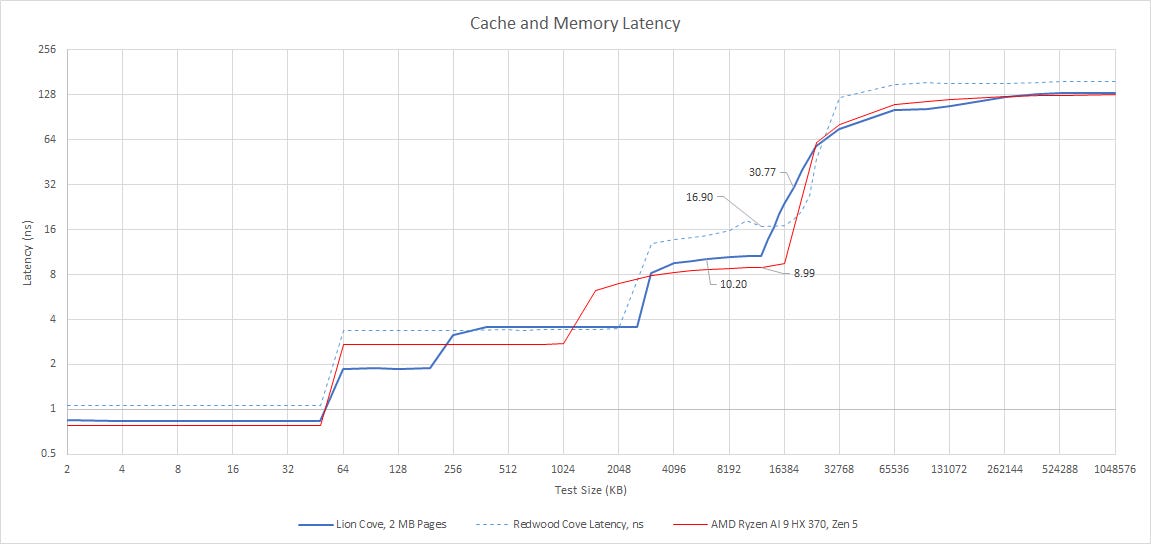
Unlike AMD Zen 5’s clustered decoder, all eight decode slots on Lion Cove can serve a single thread. Lion Cove can therefore sustain eight instructions per cycle as long as code fits within the 64 KB instruction cache. After that, code fetch throughput from L2 is limited to 16 bytes per cycle.

Longer instructions can run into cache bandwidth bottlenecks. With longer 8-byte NOPs, Lion Cove can maintain 8 instructions per cycle as long as code fits within the micro-op cache. Strangely, throughput drops well before the test should spill out of the micro-op cache. The 16 KB data point for example would correspond to 2048 NOPs, which is well within the micro-op cache’s 5250 entry capacity. I saw the same behavior on Redwood Cove.

Once the test spills into the L1 instruction cache, fetch bandwidth drops to just over 32 bytes per cycle. And once it gets into L2, Lion Cove can sustain 16 instruction bytes per cycle.

Which I thought was impossible according to Tesla engineers?

huh? what tesla engineers?

I was confused as well, though I don't see a specific quote that said it was impossible in the link below, here is an interview with a Tesla Engineer just apparently riffing on ISA variable length decode and the Mongols:


Weird.
 
I was confused as well, though I don't see a specific quote that said it was impossible in the link below, here is an interview with a Tesla Engineer just apparently riffing on ISA variable length decode and the Mongols:


Weird.

The guy’s name sounds familiar. I think we overlapped for about a year at AMD, though he was in Texas and I was in California.
 
The guy’s name sounds familiar. I think we overlapped for about a year at AMD, though he was in Texas and I was in California.
Obviously I don’t know him, but I have to admit I have an instant dislike for people who refer to “normies” derogatorily. Fetishization of autism in tech, especially in leadership qualities, generally just conflates being an asshole with being autistic and being autistic with being superior. Actual autistic people hate that shit. So that and the misunderstanding of who and what the Mongols were combined with the elevation of Musk as a great leader just reinforces to me that he’s a jackass.
 
Obviously I don’t know him, but I have to admit I have an instant dislike for people who refer to “normies” derogatorily. Fetishization of autism in tech, especially in leadership qualities, generally just conflates being an asshole with being autistic and being autistic with being superior. Actual autistic people hate that shit. So that and the misunderstanding of who and what the Mongols were combined with the elevation of Musk as a great leader just reinforces to me that he’s a jackass.
he worked on our Austin team, so he starts out in my jackass list until he proves otherwise.
 
Does the M1 8-wide decoder have these caveats?
The M1 has a much larger instruction cache - 192 KB (for all generations of M1-4 as far as I can tell), but I’ll be honest I don’t know the details of how it behaves other than decode throughput is generally easier on ARM, fixed vs variable length, but I’m not sure if the caveats above have much to do with that other than I don’t think microcode caches being as necessary for ARM (they still have them I think but as others here pointed out earlier in this thread it’s not really the same thing).
 
I don't think that's right:


You can read more about Zen5 clustered decode approach here: https://chipsandcheese.com/p/zen-5s-2-ahead-branch-predictor-unit-how-30-year-old-idea-allows-for-new-tricks

As pointed out by @data_dave, what I wrote is based on old information and the new data suggest that Zen5 does not use clustered decode to improve single-threaded performance.
 
Last edited:

Yes but in the latest papers they back off from what they said in that earlier article:

Superficially, Zen 5’s frontend looks like the ones in Intel’s latest E-Cores. However, they don’t work the same way. Each Zen 5 cluster only handles a single thread, and maximum frontend throughput can only be achieved if both SMT threads are loaded. Intel’s scheme has all clusters working in parallel on different parts of a single thread’s instruction stream. Mixing taken branches into the test for Zen 5 doesn’t improve throughput as it did with Intel’s first generation clustered decode implementation in Tremont. Therefore, Zen 5 is likely not using branches to load balance between the two decode clusters.

That's from the Strix Point article I link to above. And they repeat this again in the Zen 5 desktop article and again in the Lion Cove article. These are all written after the more theoretical article you linked to which was from before they had tested Zen 5. They go into much more depth about the actual decode strategy in the Zen 5 desktop article and attempt to explain why AMD chose this approach. Given this, they really should go back and edit or put a disclaimer on their previous, theoretical article because that one certainly makes it sound like that Zen 5 has a clustered decode approach where both clusters can be used on the same thread and their subsequent articles say that, after testing, this is definitely not the case: only a single cluster can be used on a thread.
 
Last edited:
Yes but in the latest papers they back off from what they said in that earlier article:


That's from the Strix Point article I link to above. And they repeat this again in the Zen 5 desktop article and again in the Lion Cove article. These are all written after the more theoretical article you linked to which was from before they had tested Zen 5. They go into much more depth about the actual decode strategy in the Zen 5 desktop article and attempt to explain why AMD chose this approach. Given this, they really should go back and edit or put a disclaimer on their previous, theoretical article because that one certainly makes it sound like that Zen 5 has a clustered decode approach where both clusters can be used on the same thread and their subsequent articles say that, after testing, this is definitely not the case: only a single cluster can be used on a thread.

Thanks, I should have read that article! Very interesting. So Zen5 managed to improve IPC without increasing the decode width? And Lunar Lake managed to improve the efficiency despite increasing the decode width? I find both these things surprising :)
 
Thanks, I should have read that article! Very interesting. So Zen5 managed to improve IPC without increasing the decode width? And Lunar Lake managed to improve the efficiency despite increasing the decode width? I find both these things surprising :)
Yeah they both showcase the duality that x86 designs still have a lot of possible improvement to make but also just how far x86 designs have to go. The rumors are that both AMD and Intel are trying to speed up their chip development not only because of competition with each other*, but also with ARM-based chips. So things are definitely heating up in the CPU space! I know everyone has said it before, but it bears repeating: feels so nice compared to the CPU stagnation we got in the 2010s in the PC/laptop space.

*e.g. Arrow Lake's gaming performance relative to AMD and even its own older chips is for some reason, head scratchingly bad, despite its productivity gains - seriously no one can figure it out as far as I can see as with better single thread and no SMT gaming should be better - and so Intel might have to release new desktop processors next year. Zen 6 is also supposed to come next year whereas before AMD was more on a 1.5-2 year time scale (maybe still sort of hold if it doesn't come out until December 2025).
 
I don’t think microcode caches being as necessary for ARM (they still have them I think but as others here pointed out earlier in this thread it’s not really the same thing).

I think you mean micro-op caches. x86 converts an instruction into its μop cluster equivalent and issues the μops to the EUs to be executed, which can sometimes have an out-of-order aspect to it. By using a μop cache, x86 can capture a short loop inside the core and reissue the constituent instructions in their pre-decoded form, which saves a lot of work. And code often spends significant time running short loops.

I suspect ARM mostly does not use μop caches because the decode phase is profoundly more simple than x86, so the savings is not worth the extra logic. For the lion's share of instructions, one or maybe two μops are generated in the secondary decode stage, and, despite the name, μops are much larger than the instructions that generate them, so a cache may have been determined to be wasted real estate relative to the net value it offers.

I am not entirely clear what microcode is. It has been my impression that it amounts to little programs inside the core that carry out complex functions much faster than instruction code would. Ops like enter and leave were probably originally implemented as microcode but later converted to a μop cluster. I think multiplication and division were microcoded on the 8086 but later converted to logic structures. And of course, sometimes processor flaws can be fixed by altering the microcode. But I do not think ARM has used any microcode for some while, relying on multiple μops and μop tagging instead.

In all of the chips I worked on, microcode was always just what I think you are calling micro-ops. You convert one ISA instruction to N internal instructions, and typically the translation isn’t very complicated. I think N was generally under 8, if I remember correctly. This generally was because a particular instruction might involve the LOAD/STORE unit (because it contains a memory access) as well as, say, the EX unit (e.g. any x86 instruction that does an ADD/SUBSTRACT and puts the result in RAM, or whatever). So you’d break that into an ADD that stores the result in a non-ISA register and then a STORE that reads from the non-ISA register (or bypasses the register and reads it from the output of the adder). Anyway, we always used the terminology “microcode” ourselves, though we recognized that sometimes it’s called micro-ops or various other things.
 
In all of the chips I worked on, microcode was always just what I think you are calling micro-ops. You convert one ISA instruction to N internal instructions, and typically the translation isn’t very complicated. I think N was generally under 8, if I remember correctly. This generally was because a particular instruction might involve the LOAD/STORE unit (because it contains a memory access) as well as, say, the EX unit (e.g. any x86 instruction that does an ADD/SUBSTRACT and puts the result in RAM, or whatever). So you’d break that into an ADD that stores the result in a non-ISA register and then a STORE that reads from the non-ISA register (or bypasses the register and reads it from the output of the adder). Anyway, we always used the terminology “microcode” ourselves, though we recognized that sometimes it’s called micro-ops or various other things.

So i went and looked this up, to see what’s going on. This appears to be something that academics came up with that isn’t usually a real distinction. They use “micro-op” to mean the decoded instruction. I never thought about this as an “op” of any sort. I just knew that if I was designing the integer execution unit, I received a bunch of input signals to tell the unit what to do. These would vary from design to design, not always based on what the architects defined - we would sometimes create special signals because of timing issues or the like. We never thought of these as part of an “op.”

We also wouldn’t pull all of these out of a lookup table or anything. These were generated by combinatorial logic by the decoders.

The same academics then call “microcode” the stuff that is the translation from ISA to “machine level.” But these are really the same thing in any design I’ve seen.
 
Back
Top